Si-based gallium oxide film back gate solar-blind ultraviolet ray transistor and preparation method thereof

A gallium oxide and back gate technology is applied in the field of solar-blind ultraviolet phototransistors of Si-based gallium oxide thin film back gate and their preparation, which can solve the problems of limited application scope, difficult device integration process, etc. The process is simple and the effect of avoiding the interference of noise signals

Active Publication Date: 2018-08-31
北京镓和半导体有限公司
View PDF2 Cites 16 Cited by
  • Summary
  • Abstract
  • Description
  • Claims
  • Application Information

AI Technical Summary

Problems solved by technology

Ga 2 o 3 Solar-blind detectors with heterojunctions formed by thin films and other semiconductor materials can greatly improve the performance of solar-blind photodetectors (including light responsivity, quantum efficiency, and light response speed) by using junction effects (heterojunctions, Schottky junctions, etc.) etc.), has a significant photomultiplier effect, and can detect weak optical signals. However, one end of the heterojunction device is connected to the heterogeneous substrate, and the detection function area is not independent of the substrate, which brings great advantages to the integration of the device. Difficulties in the process limit the scope of its application

Method used


Image

  • Si-based gallium oxide film back gate solar-blind ultraviolet ray transistor and preparation method thereof
  • Si-based gallium oxide film back gate solar-blind ultraviolet ray transistor and preparation method thereof
  • Si-based gallium oxide film back gate solar-blind ultraviolet ray transistor and preparation method thereof

Examples


preparation example Construction

[0033] The preparation method of the Si-based gallium oxide film back gate solar-blind ultraviolet phototransistor comprises the following steps:

[0034] The first step, substrate pretreatment;

[0035] First take a piece of p-Si / SiO 2 (Si thickness is 0.5mm, resistivity is 5-10Ω·cm; SiO 2 Thickness is 300nm) as the substrate (purchased from Hefei Yuanjing Technology Materials Co., Ltd.), p-Si / SiO 2 Soak the substrate in acetone, ethanol, and deionized water in turn for 15 minutes, rinse with deionized water after taking it out, and finally dry it with dry argon, and set it aside;

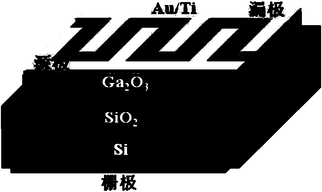
[0036] The second step, in p-Si / SiO 2 Substrate SiO 2 A photosensitive layer is prepared on the layer.

[0037] The above cleaned p-Si / SiO 2 substrate into the deposition chamber, the SiO 2 Growth of β-Ga on the side of the insulating gate layer 2 o 3 film. The adopted method includes magnetron sputtering, molecular beam epitaxy, pulse laser deposition or sol-gel method, and the thicknes...

Embodiment 1

[0043] First take a piece of p-Si / SiO with a size of 5mm×4mm 2 Substrate (Si thickness is 0.5mm, SiO 2 The thickness is 300nm) soaked in acetone, ethanol, and deionized water for 15 minutes respectively, rinsed with deionized water after taking it out, and finally dried with dry argon, and set aside.

[0044] The above cleaned p-Si / SiO 2 The substrate was placed in the deposition chamber, and the SiO 2 A layer of gallium oxide film of about 500nm is grown on the layer. The specific parameters of the magnetron sputtering method are as follows: the background vacuum is 1 × 10 -4 Pa, the working atmosphere is argon, the argon flow rate is 25 sccm, the working pressure is 0.8 Pa, the substrate temperature is 550°C, the sputtering power is 70W, and the sputtering time is 2h.

[0045] Cover the above-grown gallium oxide film with a hollow mask, and use the magnetron sputtering method to successively sputter a metal Ti electrode layer (about 6nm) and an Au electrode layer (about ...


PUM


Abstract

The invention discloses a Si-based gallium oxide film back gate solar-blind ultraviolet ray transistor and a preparation method thereof, and belongs to the photoelectric detector and semiconductor transistor technical field; the transistor comprises the following parts arranged from bottom to top in sequence: a back gate electrode layer, a substrate layer, a light-sensitive layer and an interdigital electrode layer; the substrate employs a p-Si / SiO2, and a gallium oxide film is prepared and grown on a SiO2 layer of the p-Si / SiO2 substrate so as to serve as the light-sensitive layer; an Au / Ti electrode is sputtered on the gallium oxide film so as to form the interdigital electrode; a metal Au film is sputtered on the Si layer of the backside of the p-Si / SiO2 substrate so as to serve as theback gate electrode. The preparation process is simple, and a silicon base device can be easily integrated; the method is strong in controllability, easy to operate, and the obtained film is compact in surface, even and stable in thickness, good in repeatability, easy to integrate, and can be massively made; the prepared device structure can be regulated and controlled by the gate voltage so as toobtain high solar-blind ultraviolet ray current gains.

Description

technical field [0001] The invention belongs to the technical field of photodetectors and semiconductor transistors, and in particular relates to a solar-blind ultraviolet phototransistor with a Si-based gallium oxide film back gate and a preparation method thereof. Background technique [0002] The ozone layer in the atmosphere has a strong absorption effect on ultraviolet light with a wavelength between 200nm and 280nm. The ultraviolet radiation in this band that reaches the ground is almost attenuated to zero near sea level, which is called the solar blind zone, so it is necessary for the work The solar-blind photodetector system in this band provides a good signal background. With the development of solar-blind ultraviolet detection technology, there are more and more applications in military and civilian fields, such as solar-blind ultraviolet communication, missile early warning tracking, rocket tail flame detection, space-based ultraviolet early warning, ultraviolet h...

Claims


Application Information

Patent Timeline
Patent Type & Authority Applications(China)
IPC IPC(8): H01L21/02H01L31/18H01L31/032H01L31/113
CPCH01L21/02381H01L21/02414H01L21/02428H01L21/02565H01L21/02609H01L21/02631H01L31/032H01L31/1136H01L31/18Y02P70/50
Inventor 唐为华崔尉彭阳科陈政委郭道友吴真平
Owner 北京镓和半导体有限公司
Why Eureka
Try Eureka