Double-gate organic thin film transistor and preparation method thereof
An organic thin film and transistor technology, applied in the field of organic thin film transistor preparation, can solve problems such as poor capacitance effect, no transistor performance, damage, etc., to improve processing resolution and speed, improve top gate control capability, and reduce manufacturing costs. Effect
- Summary
- Abstract
- Description
- Claims
- Application Information
AI Technical Summary
Problems solved by technology
Method used
Image

Examples
preparation example Construction
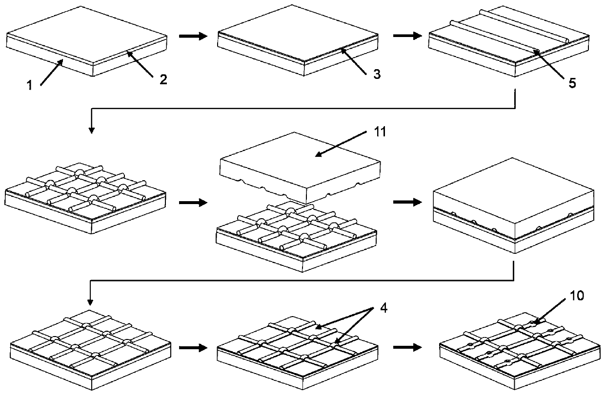
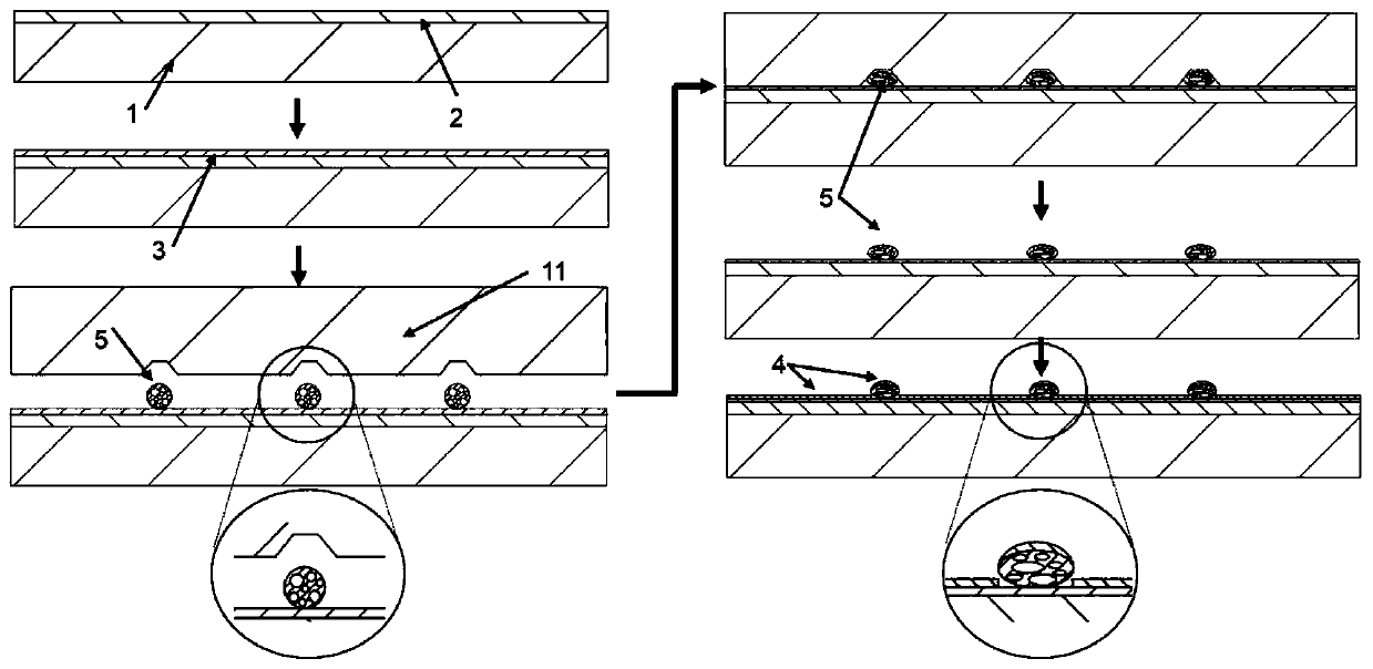
[0037] A method for preparing a double-gate organic thin film transistor provided in an embodiment of the present invention, such as figure 1 with figure 2 shown, including the following steps:
[0038] S1 prepares the bottom gate electrode 1, the bottom gate dielectric layer 2 and the active layer 3, specifically including the following steps:
[0039] (1) Prepare a conductive layer on a substrate made of a rigid material or a flexible material, and the conductive layer is the bottom gate electrode 1;
[0040] (2) Depositing a layer of insulating film on the bottom gate electrode 1 as the bottom gate dielectric layer 2 by atomic layer deposition;
[0041] (3) A semiconductor solution prepared with an organic semiconductor material is used to form a semiconductor film on the bottom gate dielectric layer 2 as the active layer 3 by spin coating, electrospray printing or electrospray. Specifically, the organic semiconductor material is a conjugated polymer or small molecule m...
Embodiment 1
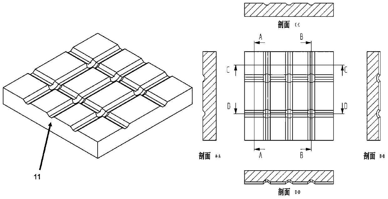
[0057] Rigid substrate silicon wafers are used to prepare silicon-based centralized control dual-gate organic thin film transistors, such as Figure 5 shown, including the following steps:
[0058] S1 Preparation of bottom gate electrode 1, bottom gate dielectric layer 2 and active layer 3:
[0059] (1) Scribe a silicon wafer: the substrate is a single-sided polished silicon oxide wafer with a surface oxidation thickness of 300nm, which can be directly used as the bottom gate electrode 1 and the bottom gate dielectric layer 2, and the silicon wafer is scribed to a size of 1cm×cm;
[0060] (2) Silicon wafer cleaning: place the silicon wafer in a mixed solution of 16ml of concentrated sulfuric acid (98%) and 8ml of hydrogen peroxide (30%), slowly heat to 100°C for 30 minutes and then slowly cool down to room temperature, thereby removing the surface of the silicon wafer Easy to oxidize and not resistant to acid impurities; then rinse the silicon wafer with running water to remo...
Embodiment 2
[0070] Using flexible substrate polyimide film (PI film) to prepare flexible PI film substrate independently controlled dual-gate organic thin film transistors, such as Image 6 shown, including the following steps:
[0071] S1 Preparation of bottom gate electrode 1, bottom gate dielectric layer 2 and active layer 3:
[0072] (1) Cutting and cleaning the PI film: use an ultrasonic cleaning machine with an ultrasonic power of 70W, perform ultrasonication on deionized water for 10 minutes, acetone ultrasonication for 10 minutes, isopropanol ultrasonication for 10 minutes, ethanol ultrasonication for 10 minutes, and deionized water ultrasonication for 10 minutes to remove other components on the surface of the PI film. Impurities are finally blown dry with nitrogen, and placed in an oven at 70°C for 10 minutes before use;
[0073] (2) Preparation of bottom gate electrode 1: PI thin film is used as flexible substrate 13, and since it does not have conductivity, patterned bottom g...
PUM
| Property | Measurement | Unit |
|---|---|---|
| diameter | aaaaa | aaaaa |
| thickness | aaaaa | aaaaa |
| thickness | aaaaa | aaaaa |
Abstract
Description
Claims
Application Information
 - R&D Engineer
- R&D Manager
- IP Professional
- Industry Leading Data Capabilities
- Powerful AI technology
- Patent DNA Extraction
Browse by: Latest US Patents, China's latest patents, Technical Efficacy Thesaurus, Application Domain, Technology Topic.
© 2024 PatSnap. All rights reserved.Legal|Privacy policy|Modern Slavery Act Transparency Statement|Sitemap