Method for preparing two-dimensional material by stripping layered material with oxide semiconductor nano-powder

A technology of oxide semiconductors and nanopowders, which is applied in the direction of oxide/hydroxide preparation, sulfide/polysulfide preparation, chemical instruments and methods, etc., which can solve the randomness of the stripping method and the fluctuation of process parameters Problems such as chemical vapor deposition and small molecule synthesis preparation, to achieve the effect of low light efficiency

Inactive Publication Date: 2021-01-01
NORTHWESTERN POLYTECHNICAL UNIV
View PDF4 Cites 8 Cited by
  • Summary
  • Abstract
  • Description
  • Claims
  • Application Information

AI Technical Summary

Problems solved by technology

Although many two-dimensional materials can also be prepared by chemical vapor deposition and small molecule synthesis, many two-dimensional materials, such as black phosphorus (b-P), black arsenic phosphide (b-As x P 1-x ), metal oxide MoO 3 , mica, TaS 2 , LDHs and TiS 2 etc., but cannot be prepared by chemical vapor deposition and small molecule synthesis, and can only be easily prepared by a top-down exfoliation method
Therefore, the top-down exfoliation method to obtain its two-dimensional structure is a more general method, but the existing exfoliation methods have randomness and process parameter fluctuations, which cannot guarantee that the exfoliated two-dimensional materials are all single layers, and the exfoliated two-dimensional Material layers are generally in the form of single-layer and multi-layer mixtures

Method used


Image

  • Method for preparing two-dimensional material by stripping layered material with oxide semiconductor nano-powder

Examples


Embodiment 1

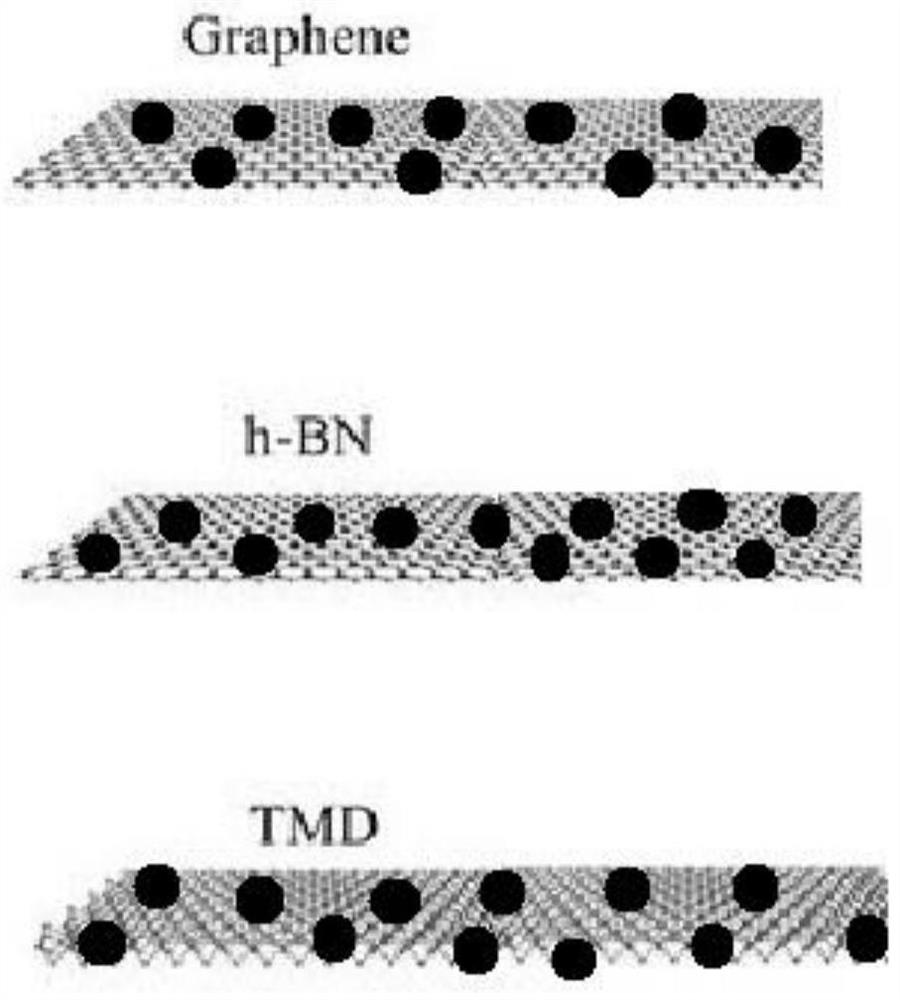
[0109] Example 1: Manganese nitrate, ferric nitrate and nickel nitrate solutions are mixed according to the atomic equivalent of the three metal elements 3:1:1, then precipitated with ammonia water, sintered and decomposed at high temperature in the air to form p-type semiconductor nanopowder of oxide solid solution The specific preparation of p-type semiconductor powder does not belong to the scope of protection of this patent. This is just an example, and the specific preparation method is not limited, as long as it is a semiconductor nanoparticle smaller than 100nm and forms an oxygen-deficient p-type semiconductor powder. Conductivity is enough. The work function of this semiconductor is about 4.7eV, which is greater than the work function of the two-dimensional material molybdenum disulfide, which is about 1.9eV. The specific proportion of transition metal manganese-iron-nickel oxide nanoparticles is 50 grams, mixed with 0.5 grams of few-layer molybdenum disulfide , the m...

Embodiment 2

[0110]Embodiment 2: The NiO oxide solid solution is a p-type semiconductor nanopowder. The work function of this nickel oxide semiconductor is greater than the work function of the two-dimensional material graphite, and 100 grams of nickel oxide nanoparticles with a specific ratio of about 30 nm particle size are mixed with 0.5 grams of graphite powder, and the mass ratio of the two (1:130 ) is greater than 1:25, then in a grinder, grind for 16 hours in an inert gas argon protective atmosphere, observe with an electron microscope, the nanoparticles have absorbed more than 99% of single-layer or few-layer graphene, and the grinding is over; if the observation does not reach the nanometer The particles adsorb more than 90% of single-layer or few-layer graphene, and continue to grind until reaching. Taking out the composite intermediate structure with nanoparticles adsorbed on the surface of graphene can be used for specific purposes. Then add the composite intermediate to an aq...

Embodiment 3

[0111] Embodiment 3: Manganese oxide, copper oxide and cobalt oxide powders are ground according to the atomic equivalent of three metal elements 3:1:3 mixed ball mill, and then the solid solution oxide p-type semiconductor nano-powder made by sintering at high temperature is specifically prepared. Powder does not belong to the protection scope of this patent, and it is just an example here. The work function of this oxide solid solution semiconductor is about 4.6eV, which is greater than that of MXene (titanium carbide) at about 1.7-1.9eV. The specific ratio of transition metal manganese-iron-nickel oxide nanoparticles is 20 grams, and the few-layer molybdenum disulfide Mix 0.25 grams, the mass ratio (1:80) of the two is greater than 1:25, and then grind for 8 hours in an inert gas argon protective atmosphere in a planetary grinder, and observe with an electron microscope, the nanoparticles have adsorbed more than 99% of the monolayer or Few layers of MXene (titanium carbide)...


PUM

PropertyMeasurementUnit
specific surface areaaaaaaaaaaa
particle diameteraaaaaaaaaa

Abstract

The invention relates to a method for preparing a two-dimensional material by stripping a layered material with oxide semiconductor nano-powder. The method comprises the following steps: adsorbing p-type semiconductor nano-particles containing oxygen vacancies (oxygen holes) on the surface of the layered material while reactively adsorbing the semiconductor nano-particles on the surface of the layered material, and carrying out grinding in a grinder to realize inter-layer separation, carrying out stripping to prepare the two-dimensional material which is an intermediate film formed by compounding a single-layer or few-layer atom or molecular layer two-dimensional material and nanoparticles. and then separating the nanoparticles from the two-dimensional film to obtain the two-dimensional material. According to the technology, two types of practical products can be obtained, one type is an intermediate film formed by compounding a single-layer or few-layer atom or molecular layer two-dimensional material and nanoparticles; the other type is a two-dimensional material, and the two types of materials have wide and special applications.

Description

technical field [0001] The invention belongs to a method for preparing a two-dimensional material, and relates to a method for preparing a two-dimensional material by exfoliating a layered material from an oxide semiconductor nanopowder, involving the use of an oxide nanoparticle containing an oxygen-deficient p-type semiconductor, and a layered material Grinding and compounding to peel off the layered material to prepare a composite intermediate structure whose surface is covered with p-type oxide semiconductor nanoparticles and covered with a few-layer two-dimensional material surface, and then eluted with a salt solution to obtain a single-layer or few-layer Methods for 2D materials. The prepared two-dimensional materials and intermediate composite structures have potential applications in a wide range of fields, including electronic / optoelectronic devices, semiconductors, flexible electronics, electronic backgrounds and electronic displays, electrocatalytic reactions, batt...

Claims


Application Information

Patent Timeline
Patent Type & Authority Applications(China)
IPC IPC(8): C01G39/06C01B32/19C01B32/921C01B19/04C01B25/02C01B17/20C01B32/90C01B21/06C01B35/02C01B21/064C01B21/082C01B13/14B22F9/04C07C209/86C07C211/04
CPCC01G39/06C01B32/19C01B32/921C01B19/007C01B19/04C01B25/02C01B17/20C01B32/90C01B21/06C01B35/023C01B21/0648C01B21/0605C01B13/14B22F9/04C07C209/86C01B2204/02C01P2004/20C07C211/04
Inventor 苏力宏王锡桐王波锁永永阿克卓理·切尔扎提安立闫方圆黄维
Owner NORTHWESTERN POLYTECHNICAL UNIV
Why Eureka
Try Eureka