Nanorod-shaped antimonous sulfide electromagnetic wave absorbing material, absorber, preparation method and application
A technology of antimony trisulfide and nano-rods, which is applied in chemical instruments and methods, polycrystalline material growth, electrical components, etc., can solve the problems of increasing the reflection of electromagnetic waves by materials, reducing the efficiency of electromagnetic wave absorption, and insufficient loss capacity, etc., to achieve Unique microscopic morphology, improved bulk polarization relaxation loss capability, and increased direct contact effect
- Summary
- Abstract
- Description
- Claims
- Application Information
AI Technical Summary
Problems solved by technology
Method used
Image
Examples
preparation example Construction
[0039] In a third aspect, the present invention provides a method for preparing the nanorod-shaped antimony trisulfide electromagnetic wave absorbing material, comprising the following steps:
[0040] Solvothermal reaction of mixed solution of antimony source and sulfur source to prepare nanorod-like Sb 2 S 3 Electromagnetic wave absorbing materials;
[0041] The antimony source is antimony chloride (SbCl 3 ), antimony nitrate (Sb(NO 3 ) 3 ) or antimony acetate (Sb(CH 3 COO) 3 ) in any one or a mixture of two or more;
[0042] The sulfur source is sodium sulfide (Na 2 S), potassium sulfide (K 2 S), thioacetamide (C 3 h 7 NO 2 S) or L-cysteine (C 3 h 7 NO 2 S).
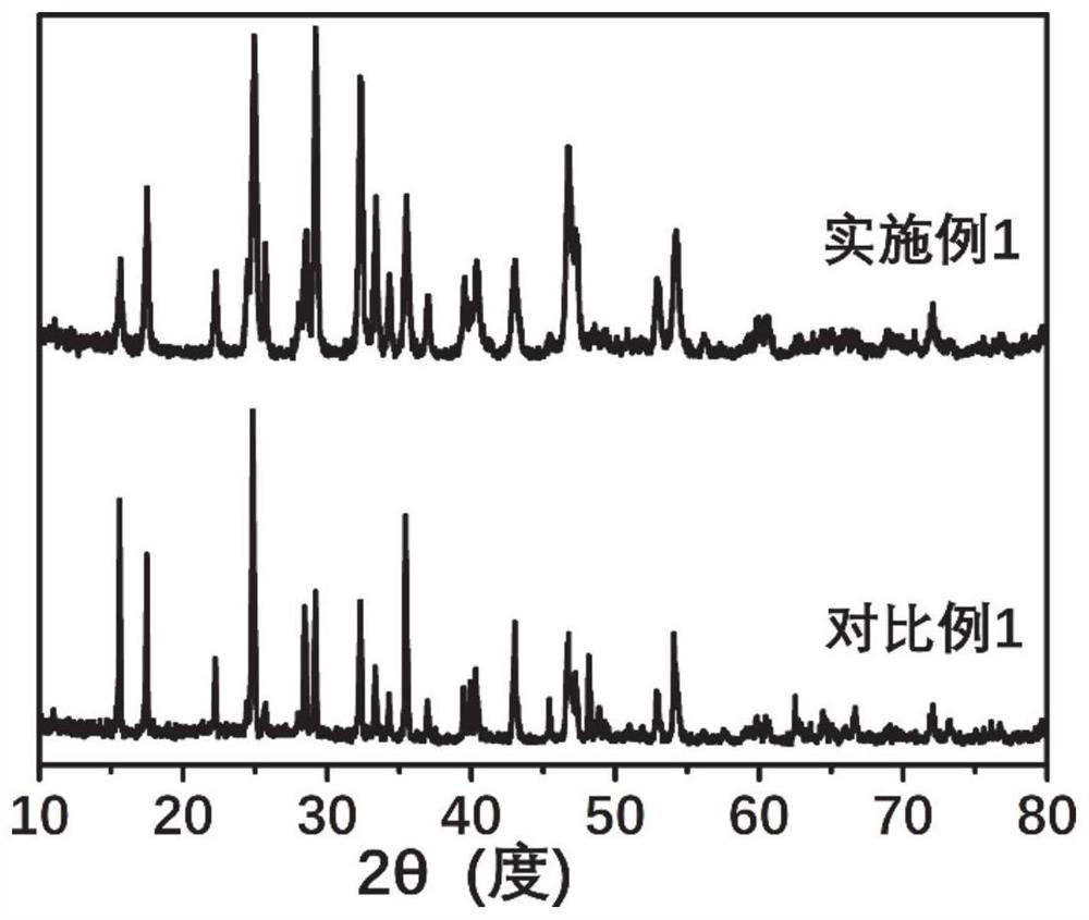
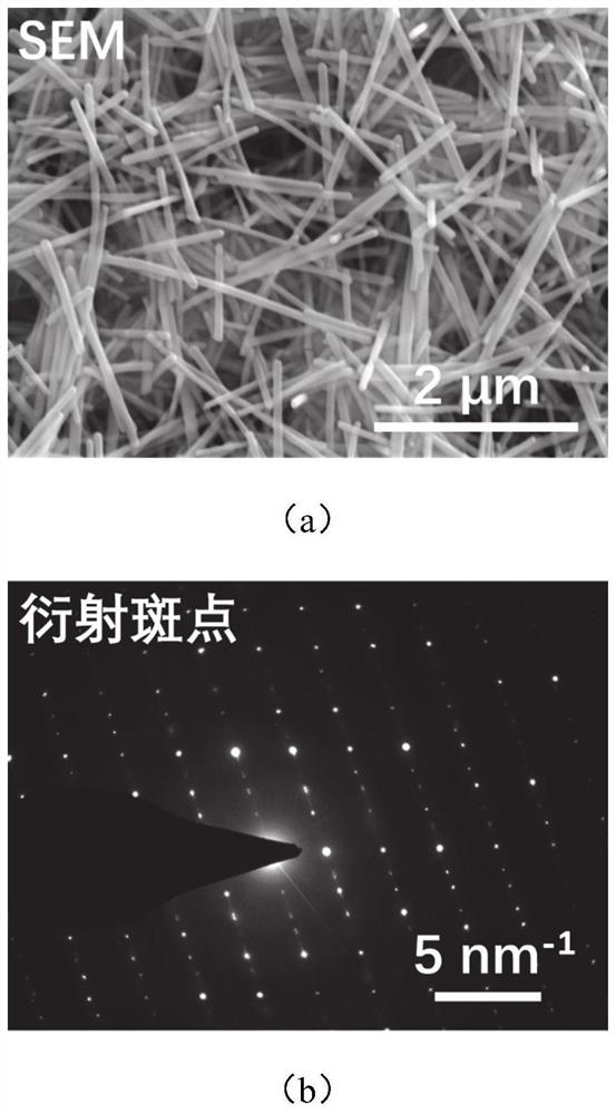
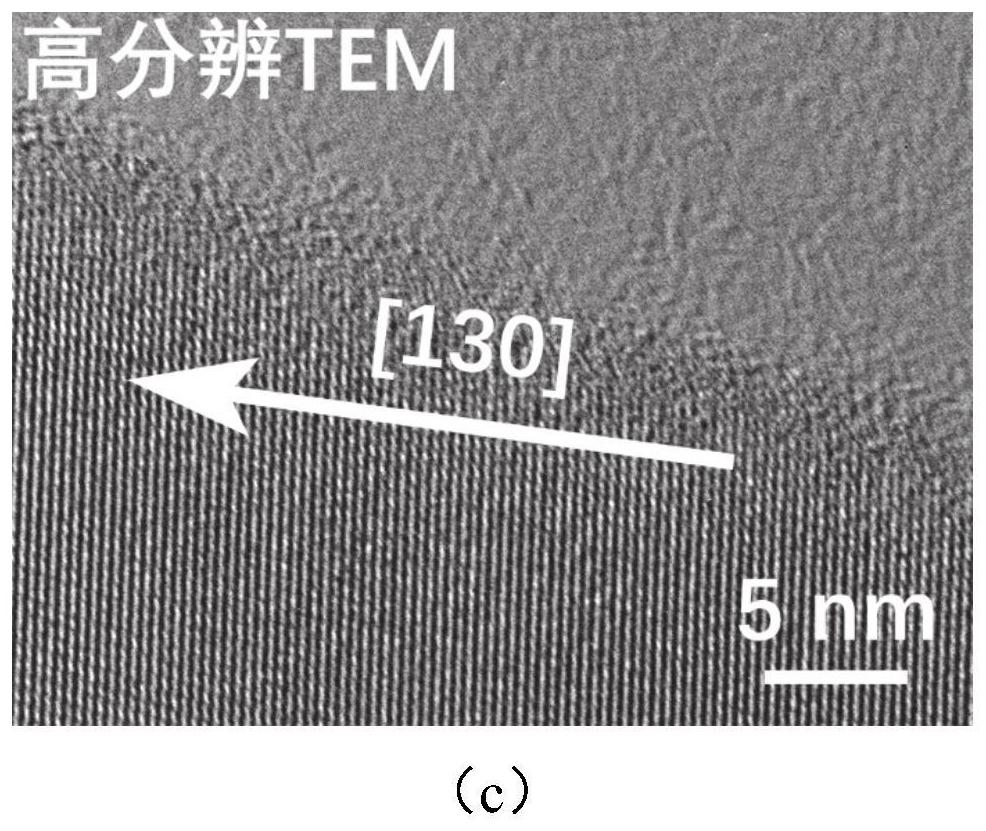
[0043] This preparation method utilizes a special sulfur source as a reactant and a surfactant to regulate the solution surface properties of the reaction environment at the same time, so that Sb 2 S 3 In the process of formation and growth, the [130] direction is the preferential growth direction of...
Embodiment 1
[0052] A nanorod-like Sb 2 S 3 The preparation method of the filled electromagnetic wave absorber comprises the following steps:
[0053] (1) 2.5mmol SbCl 3 , 5.0 mmol C 3 h 7 NO 2 S and 5.0 mmol Na 2 S was successively dissolved in 50.0 mL of deionized water and stirred continuously for 3 h until a homogeneous solution was obtained.
[0054] (2) Transfer all the solution in step (1) to a polytetrafluoroethylene-lined steel reaction kettle, and heat to 200° C. for 2 h. The obtained solid product was centrifuged, washed several times with ethanol / water mixture, and then dried under vacuum at 60° C. for 12 h.
[0055] (3) After the solid paraffin is melted at a temperature above 75° C., mixed with an equal mass of the solid product in step (2), stirred rapidly, cooled to room temperature, and pressed into an absorber.
Embodiment 2
[0057] A nanorod-like Sb 2 S 3 The preparation method of the filled electromagnetic wave absorber comprises the following steps:
[0058] (1) 2.5mmol Sb(CH3COO) 3 and 10.0 mmol C 3 h 7 NO 2 S was successively dissolved in 50.0 mL of deionized water and stirred continuously for 3 h until a homogeneous solution was obtained.
[0059] (2) Transfer all the solution in step (1) to a polytetrafluoroethylene-lined steel reaction kettle, and heat to 200° C. for 4 h. The obtained solid product was centrifuged, washed several times with ethanol / water mixture, and then dried under vacuum at 60° C. for 12 h.
[0060] (3) After the solid paraffin is melted at a temperature above 75° C., mixed with an equal mass of the solid product in step (2), stirred rapidly, cooled to room temperature, and pressed into an absorber.
PUM
| Property | Measurement | Unit |
|---|---|---|
| diameter | aaaaa | aaaaa |
| length | aaaaa | aaaaa |
Abstract
Description
Claims
Application Information


