
Nitrogen polar surface GaN material and homoepitaxial growth method

A nitrogen polar, epitaxial layer technology, applied in semiconductor devices, electrical components, circuits, etc., can solve the problem of increasing the background doping concentration of nitrogen polar GaN materials, hindering the migration ability and diffusion length of metal atoms, and increasing the growth process. Control difficulty and parasitic contamination to enhance migration capability and diffusion length, avoid short pauses and gaps, and reduce surface pit-like defect density

Pending Publication Date: 2021-05-04
XIDIAN UNIV
View PDF5 Cites 0 Cited by
  • Summary
  • Abstract
  • Description
  • Claims
  • Application Information

AI Technical Summary

Problems solved by technology

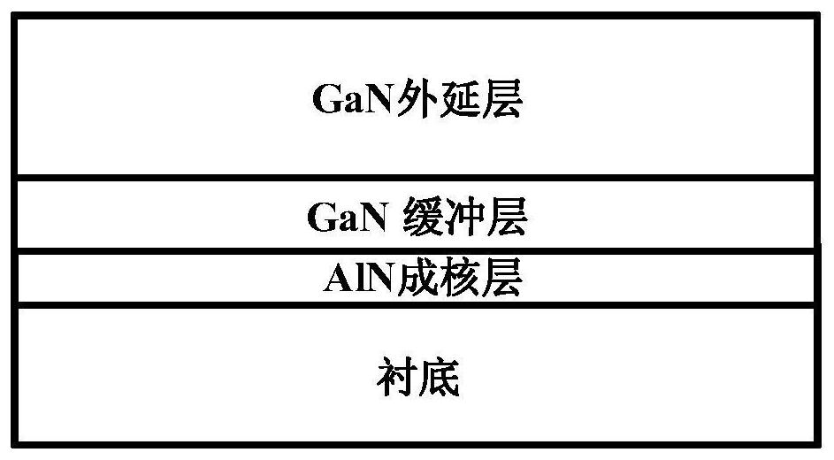
[0004] One is that there are high-density dislocation defects in the heteroepitaxial nitrogen polar surface GaN material, which will cause the degradation of device reliability, the surface of the material is rough, and there are many pit-like defects;
[0005] Second, heteroepitaxial nitrogen polar surface GaN materials are prone to polarity reversal, and polarity control is difficult;
[0006] The third is that the background carrier concentration of the heteroepitaxial nitrogen polar surface GaN material is high, which will form a bulk leakage channel and reduce the breakdown voltage of the device;
[0007] Fourth, metal-organic chemical vapor deposition technology heterogeneous epitaxial nitrogen polar surface GaN material requires the use of oblique cut substrates, which increases the cost of material epitaxy;
[0008] Fifth, metal-organic chemical vapor deposition technology heteroepitaxial nitrogen polar surface GaN material requires nitrogen-rich growth conditions, which hinder the migration ability and diffusion length of metal atoms on the film growth surface
[0009] Sixth, metal-organic chemical vapor deposition technology heterogeneous epitaxial nitrogen polar surface GaN materials need to use Fe doping to compensate the background carriers, which increases the difficulty of growth process control and parasitic pollution
[0010] Seventh, when heterogeneous epitaxial nitrogen polar surface GaN material, AlN nucleation layer and GaN buffer layer growth need to change the growth temperature and switch gas flow, the growth process requires a short pause and interval, which will increase the background of the nitrogen polar surface GaN material Doping impurity concentration

Method used


Image

  • Nitrogen polar surface GaN material and homoepitaxial growth method
  • Nitrogen polar surface GaN material and homoepitaxial growth method
  • Nitrogen polar surface GaN material and homoepitaxial growth method

Examples


Embodiment 1

[0031] Example 1, the substrate is a non-beveled gallium nitride single crystal with a nitrogen polar surface, and the transition layer is In with a thickness of 10 nm. 0.17 Al 0.83 N, the epitaxial layer is a GaN material with a nitrogen polar surface of GaN.

[0032] In step 1, a gallium nitride single crystal with a non-bevelled nitrogen polar surface is selected as the substrate, such as image 3 (a).

[0033] Step 2, epitaxy In 0.17 Al 0.83 N transition layers, such as image 3 (b).

[0034] Epitaxy of In with a thickness of 10 nm on a GaN single crystal substrate with a nitrogen polar surface using molecular beam epitaxy 0.17 Al 0.83 N transition layer.

[0035] Epitaxial In 0.17 Al 0.83 The process conditions used for the N transition layer are as follows: the temperature is 670°C, the flow rate of nitrogen gas is 2.3 sccm, and the equilibrium vapor pressure of the indium beam is 1.5×10 -7 Torr, the equilibrium vapor pressure of an aluminum beam is 2.3×10 -7...

Embodiment 2

[0039] Example 2, the substrate is a non-beveled gallium nitride single crystal with a nitrogen polar surface, and the transition layer is Sc with a thickness of 5 nm. 0.18 Al 0.82 N, the epitaxial layer is a GaN material with a nitrogen polar surface of GaN.

[0040] In step 1, a gallium nitride single crystal with a non-bevelled nitrogen polar surface is selected as the substrate, such as image 3 (a).

[0041] Step 2, using molecular beam epitaxy to deposit Sc 0.18 Al 0.82 N transition layers, such as image 3 (b).

[0042] The set temperature is 690°C, the nitrogen flow rate is 2.3 sccm, and the scandium beam equilibrium vapor pressure is 1.3×10 -8 Torr, the equilibrium vapor pressure of an aluminum beam is 2.0×10 -7 Torr, the process condition of nitrogen RF source power is 375W, using molecular beam epitaxy technology, depositing Sc with a thickness of 5nm on the nitrogen polar surface gallium nitride single crystal substrate 0.18 Al 0.82 N transition layer.

...

Embodiment 3

[0045] Example 3, the substrate is a non-beveled gallium nitride single crystal with a nitrogen polar surface, and the transition layer is a Y layer with a thickness of 1 nm. 0.11 Al 0.89 N, the epitaxial layer is a GaN material with a nitrogen polar surface of GaN.

[0046] In step A, a gallium nitride single crystal with a non-bevelled nitrogen polar surface is selected as the substrate, such as image 3 (a).

[0047] Step B, grow Y 0.11 Al 0.89 N transition layers, such as image 3 (b).

[0048] Using molecular beam epitaxy technology, at a temperature of 720°C, a nitrogen flow rate of 2.3 sccm, and an yttrium beam equilibrium vapor pressure of 1.0×10 -8 Torr, the equilibrium vapor pressure of an aluminum beam is 2.6×10 -7 Torr, under the process conditions of nitrogen RF source power of 375W, Y with a thickness of 1nm was grown on a non-beveled nitrogen polar GaN single crystal substrate 0.11 Al 0.89 N transition layer.

[0049] Step C, growing a GaN epitaxial la...


PUM

PropertyMeasurementUnit
Thicknessaaaaaaaaaa

Abstract

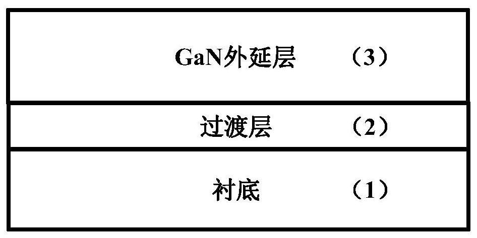
The invention discloses a nitrogen polar surface GaN material and a manufacturing method thereof, and solves the problems that an existing nitrogen polar surface GaN material is high in dislocation density, poor in surface appearance, high in unintentional doping background carrier concentration and large in growth process control difficulty are mainly solved. The nitrogen polar surface GaN material structure comprises a substrate (1), a transition layer (2) and a GaN epitaxial layer (3) from bottom to top, wherein the transition layer adopts InAlN or ScAlN or YAlN, and the substrate is made of non-diagonal plane nitrogen polar surface gallium nitride single crystal. The manufacturing method comprises the following steps of: growing the transition layer with the thickness of 1-10 nm on the substrate by using a molecular beam epitaxy method; and growing the GaN epitaxial layer on the transition layer by using the molecular beam epitaxy method. The nitrogen polar surface GaN material is high in crystallization quality, smooth in surface appearance, low in background carrier concentration, simple in growth process and high in process repeatability and consistency, and can be used for manufacturing high-electron-mobility transistors and high-speed microwave rectifier diodes.

Description

technical field [0001] The invention belongs to the field of semiconductor material growth, and particularly relates to a GaN semiconductor material with a nitrogen polarity surface, which can be used for making high-electron mobility transistors and high-speed microwave rectifier diodes. Background technique [0002] Group III nitride semiconductor materials have unique advantages in the fields of high frequency, high power, high efficiency, high temperature resistance, high pressure resistance, and radiation resistance, and are suitable for the preparation of solid-state microwave power devices and microwave millimeter wave monolithic integrated circuits. After nearly three decades of in-depth research, the performance and reliability of GaN-based high electron mobility transistors have been improved, and they have been applied in 5G communication base stations and radar detection. At present, the research and application of nitride semiconductor materials and devices are ...

Claims


Application Information

Patent Timeline
IPC IPC(8): H01L21/02H01L29/20H01L29/778H01L29/861
CPCH01L21/02389H01L21/02458H01L21/0254H01L21/02631H01L29/2003H01L29/778H01L29/861
Inventor 薛军帅李蓝星姚佳佳杨雪妍孙志鹏张赫朋刘芳张进成郝跃
Owner XIDIAN UNIV
Learn More