Preparation method of gallium oxide Schottky diode with low turn-on voltage

A Schottky diode and turn-on voltage technology, applied in circuits, electrical components, semiconductor/solid-state device manufacturing, etc., can solve the problems of high turn-on voltage, fast switching speed, low turn-on voltage, etc. On-resistance, the effect of reducing work function difference

Active Publication Date: 2021-11-02
XIDIAN UNIV
View PDF4 Cites 0 Cited by
  • Summary
  • Abstract
  • Description
  • Claims
  • Application Information

AI Technical Summary

Problems solved by technology

Although the turn-on voltage of this diode is lower than that of the pn diode, the turn-on voltage of the traditional gallium oxide Schottky diode used in high-frequency circuits is still high, which still cannot meet the low turn-on voltage, fast switching speed, and low energy loss. needs

Method used


Image

  • Preparation method of gallium oxide Schottky diode with low turn-on voltage
  • Preparation method of gallium oxide Schottky diode with low turn-on voltage
  • Preparation method of gallium oxide Schottky diode with low turn-on voltage

Examples


Embodiment 1

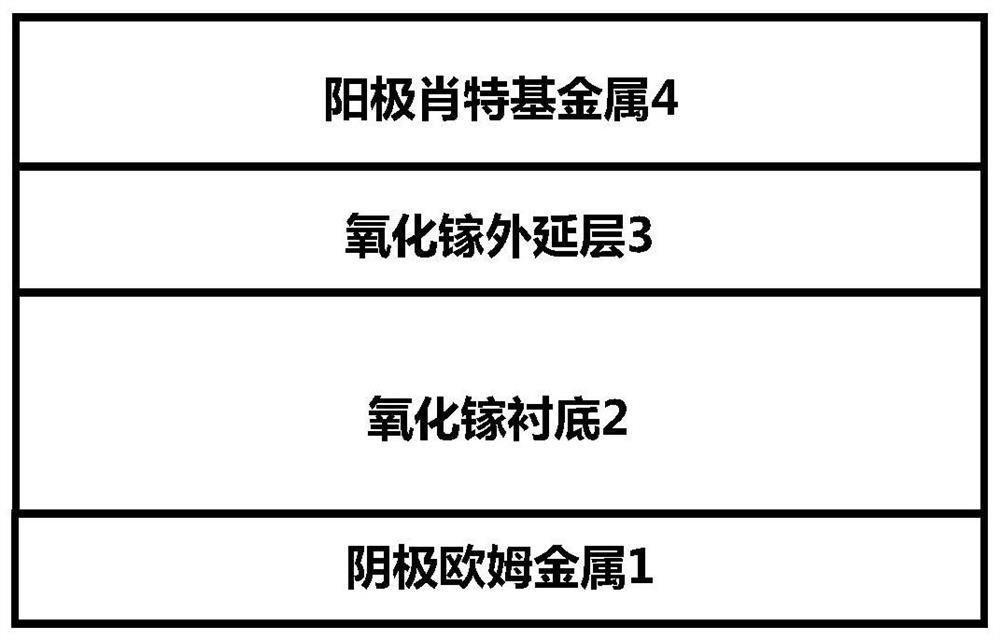
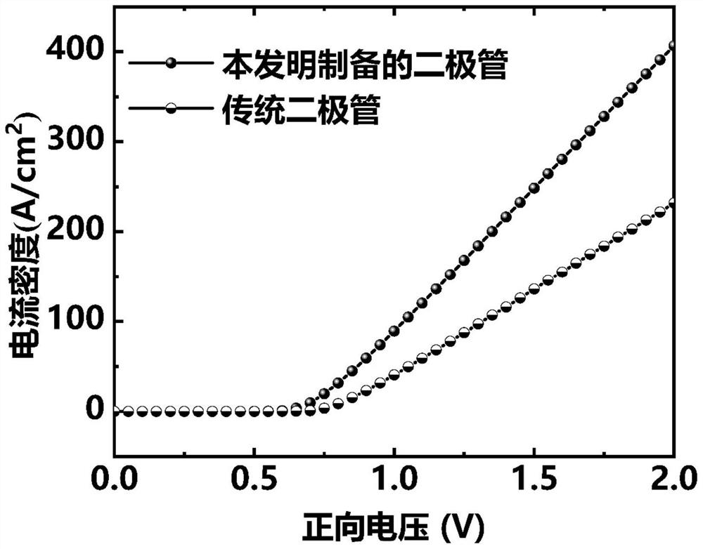
[0028] Embodiment 1: The thickness of the gallium oxide substrate is made to be 650 μm, and the effective doping carrier concentration is 10 18 cm -3 . The thickness of the lightly doped gallium oxide epitaxial layer is 10 μm, and the doping carrier concentration is 10 16 m -3 . Gallium oxide Schott for epitaxial layer gallium oxide (3) treated with laughing gas inductively coupled plasma under the conditions of power of 100W, nitrogen gas flow rate of 40sccm, pressure of 8mtorr, ambient temperature of 25°C, and treatment time of 2 minutes base diode.

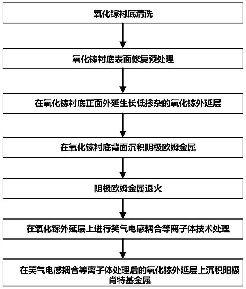
[0029] Step 1: Gallium oxide substrate cleaning.

[0030] The gallium oxide substrate 2 is selected to have a thickness of 650 μm and an effective doping carrier concentration of 10 18 cm -3 , the doping ion species is Sn ion.

[0031] Use acetone-isopropanol-deionized water to sonicate for 5 minutes respectively, and then blow dry with nitrogen.

[0032] Step 2: performing repair pretreatment on the surface of the gal...

Embodiment 2

[0048] Embodiment 2: The thickness of the gallium oxide substrate is 300 μm, and the effective doping carrier concentration is 10 20 cm -3 , the thickness of the lightly doped gallium oxide epitaxial layer is 3 μm, and the doping carrier concentration is 10 17 m -3 . Under the conditions of power of 200W, nitrogen gas flow rate of 60sccm, pressure of 10mtorr, ambient temperature of 50°C, and treatment time of 4 minutes, epitaxial layer gallium oxide (3) was treated with laughing gas inductively coupled plasma. Teky diode.

[0049] Step 1: Gallium oxide substrate cleaning.

[0050] The selected thickness is 300 μm, and the effective doping carrier concentration is 10 20 cm -3 , a gallium oxide substrate 2 doped with Sn ions as the ion type, and ultrasonically ultrasonicated for 5 minutes using acetone-isopropanol-deionized water, respectively, and then blow-dried with nitrogen gas.

[0051] Step 2: Surface restoration pretreatment on gallium oxide substrate 2 .

[0052]...

Embodiment 3

[0062] Embodiment 3: The thickness of the gallium oxide substrate is 600 μm, and the effective doping carrier concentration is 10 18 cm -3 , the doping ion type is Sn ion, the thickness of the lightly doped gallium oxide epitaxial layer is 15 μm, and the doping carrier concentration is 10 16 m -3 , and the epitaxial layer of gallium oxide (3) was treated with laughing gas inductively coupled plasma under the conditions of power of 300W, nitrogen gas flow rate of 80sccm, pressure of 12mtorr, ambient temperature of 60°C, and treatment time of 6 minutes Schottky diodes.

[0063] Step A: gallium oxide substrate cleaning.

[0064] A1) The thickness of the gallium oxide substrate is selected as 600 μm, and the effective doping carrier concentration is 10 18 cm -3 , the dopant ion type is Sn ion;

[0065] A2) Use acetone-isopropanol-deionized water to sonicate for 5 minutes respectively, and then blow dry with nitrogen gas.

[0066] Step B: Pretreatment of the gallium oxide su...


PUM

PropertyMeasurementUnit
thicknessaaaaaaaaaa
thicknessaaaaaaaaaa
thicknessaaaaaaaaaa

Abstract

The invention discloses a preparation method of a gallium oxide Schottky diode with low turn-on voltage, which mainly solves the problem of high turn-on voltage of the gallium oxide Schottky diode manufactured by the existing method. The implementation scheme is as follows: cleaning a gallium oxide substrate; carrying out surface repair pretreatment on the surface of the cleaned gallium oxide substrate, and growing a gallium oxide epitaxial layer on the front surface of the pretreated gallium oxide substrate by adopting a hydride vapor phase epitaxy (HVPE) technology; depositing ohmic cathode metal on the back surface of the gallium oxide substrate by adopting magnetron sputtering, and performing ohmic annealing on the ohmic cathode metal; carrying out laughing gas inductively coupled plasma processing on the gallium oxide epitaxial layer, and forming an anode pattern by photoetching; and depositing Schottky anode metal by electron beam evaporation according to the anode pattern to complete device manufacturing. According to the invention, the turn-on voltage of the Schottky diode is reduced; and the electron mobility of a drift layer is improved, so that the on-resistance is reduced, and the Schottky diode can be used for high-power, high-voltage and high-frequency rectification.

Description

technical field [0001] The invention belongs to the technical field of semiconductor devices, in particular to a method for manufacturing a gallium oxide Schottky diode. [0002] technical background [0003] Gallium oxide is a third-generation new semiconductor material. Due to its large band gap of 4.6-4.9eV and high critical breakdown field strength of 8MV / cm, gallium oxide semiconductor materials can be used to prepare high-power devices. In addition, gallium oxide power devices have the advantages of high breakdown voltage, high working environment and strong radiation resistance. With the continuous advancement of modern science and technology, in the fields of communication, power electronics, signal processing, aerospace and other fields, the performance of traditional third-generation semiconductor GaN and SiC power devices can no longer meet the higher performance requirements. Under the same withstand voltage as GaN and SiC, gallium oxide power devices have lower ...

Claims


Application Information

Patent Timeline
Patent Type & Authority Applications(China)
IPC IPC(8): H01L29/24H01L29/47H01L21/329H01L29/872
CPCH01L29/24H01L29/47H01L29/872H01L29/66143Y02P70/50
Inventor 郑雪峰洪悦华何云龙张方张翔宇陆小力马晓华郝跃
Owner XIDIAN UNIV
Why Eureka
Try Eureka