Preparation method of one-dimensional single crystal germanium-based graphene plasmon nanostructure
A technology of plasmonic and nanostructures, which is applied in the field of preparation of plasmonic nanostructures, can solve problems such as the inability to study the surface plasmon effect, complexity, and poor quality of graphene, so as to avoid the transfer of graphene films process, strong plasmon effect, effect of avoiding oxidation
- Summary
- Abstract
- Description
- Claims
- Application Information
AI Technical Summary
Problems solved by technology
Method used
Image
Examples
Embodiment 1
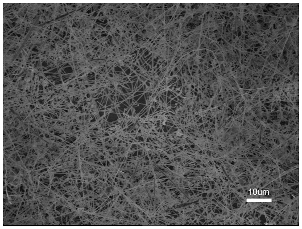
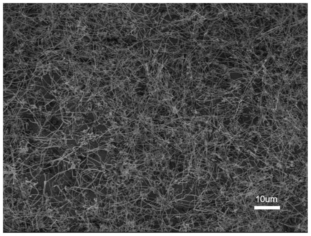
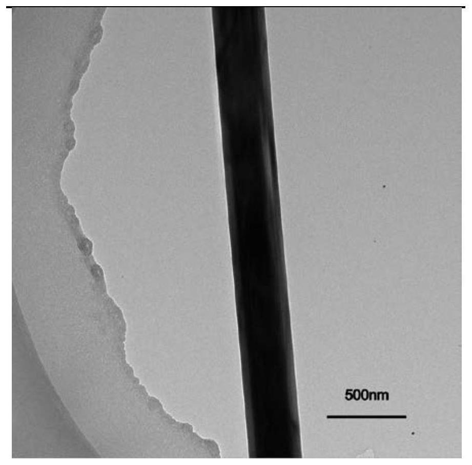
[0039] A method for preparing a one-dimensional single-crystal germanium-based graphene plasmonic nanostructure, specifically as follows:
[0040] Step 1: Cut the silicon wafer into the desired size, put it into a beaker, and use acetone solution to sonicate for 15 minutes, then put it in isopropanol solution and sonicate for 15 minutes, and finally rinse with ethanol and blow dry with a nitrogen gun for later use;
[0041] Step 2: Put the gold target and the cleaned silicon wafer into the magnetron sputtering instrument respectively, turn on the switch of the molecular pump, and let the working gas 20sccm Ar, wait until the vacuum degree of the sputtering chamber reaches 7 × 10 -4 pa, select the radio frequency mode of magnetron sputtering, set the sputtering power to 25W, set the substrate temperature to room temperature, set the sputtering time to 10s, take out the sample after sputtering, the surface of the substrate is covered with a layer of nano-scale gold film;
[004...
Embodiment 2
[0045] A method for preparing a one-dimensional single-crystal germanium-based graphene plasmonic nanostructure, specifically as follows:
[0046] Step 1: Cut the silicon wafer into the desired size, put it into a beaker, and use acetone solution to sonicate for 15 minutes, then put it in isopropanol solution and sonicate for 15 minutes, and finally rinse with ethanol and blow dry with a nitrogen gun for later use;
[0047] Step 2: Put the gold target and the cleaned silicon wafer into the magnetron sputtering instrument respectively, turn on the pump switch, and let the working gas 20sccm Ar, wait until the vacuum degree of the sputtering chamber reaches 7×10 -4 pa, select the radio frequency mode of magnetron sputtering, set the sputtering power to 25W, set the substrate temperature to 400°C, set the sputtering time to 20s, take out the sample after sputtering, the surface of the substrate is covered with a layer of nanoscale Gold film;
[0048] Step 3: Weigh 300mg of germa...
Embodiment 3
[0051] A method for preparing a one-dimensional single-crystal germanium-based graphene plasmonic nanostructure, specifically as follows:
[0052] Step 1: Cut the silicon wafer into the desired size, put it into a beaker, and use acetone solution to sonicate for 15 minutes, then put it in isopropanol solution and sonicate for 15 minutes, and finally rinse with ethanol and blow dry with a nitrogen gun for later use;
[0053] Step 2: Put the gold target and the cleaned silicon wafer into the magnetron sputtering instrument respectively, turn on the pump switch, and let the working gas 20sccm Ar, wait until the vacuum degree of the sputtering chamber reaches 7×10 -4 pa, select the radio frequency mode of magnetron sputtering, set the sputtering power to 25W, set the substrate temperature to 400°C, set the sputtering time to 10s, take out the sample after sputtering, the substrate surface is covered with a layer of nano-scale Gold film;
[0054] Step 3: Weigh 500mg of germanium p...
PUM
| Property | Measurement | Unit |
|---|---|---|
| thickness | aaaaa | aaaaa |
| length | aaaaa | aaaaa |
| diameter | aaaaa | aaaaa |
Abstract
Description
Claims
Application Information


