Antimicrobial semiconductor coating layer with detection effect and preparation method and application thereof

An anti-microbial and semiconductor technology, used in coatings, metal material coating processes, pharmaceutical formulations, etc., to avoid the use of antibiotics, achieve antimicrobial activity, and high antibacterial efficiency.

Pending Publication Date: 2022-02-18
SHENZHEN INST OF ADVANCED TECH +1
View PDF0 Cites 0 Cited by
  • Summary
  • Abstract
  • Description
  • Claims
  • Application Information

AI Technical Summary

Problems solved by technology

This clean and environmentally friendly antibacterial system overcomes the systemic side effects of existing release antibacterial surfaces and the disadvantages of refilling antibacterial substances

Method used


Image

  • Antimicrobial semiconductor coating layer with detection effect and preparation method and application thereof
  • Antimicrobial semiconductor coating layer with detection effect and preparation method and application thereof
  • Antimicrobial semiconductor coating layer with detection effect and preparation method and application thereof

Examples


preparation example Construction

[0070] Another aspect of the present invention provides a method for preparing a semiconductor coating, comprising the steps of:

[0071] 1) epoxy groups are formed on the surface of the substrate;

[0072] 2) Generate semiconductor nano-arrays on the epoxy base by hydrothermal method or anodic oxidation method;

[0073] 3) Decorate the metal nanoparticles on the surface of the semiconductor nanoarray.

[0074] In some specific embodiments of the present invention, the method for forming epoxy groups on the surface of the substrate is to react the substrate with a silane coupling agent, preferably γ-(2,3-glycidoxy)propyltrimethoxysilane, Get epoxy. The epoxy group can make the semiconductor nano-array contact more closely with the substrate, thereby strengthening the electron transfer process and improving the antibacterial effect.

[0075] In some specific embodiments of the present invention, the method of generating zinc oxide semiconductor nano-arrays on the epoxy group...

Embodiment 1

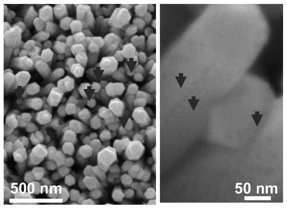
[0104] The titanium alloy is processed into cuboids with a length, width and height of 30 mm, 30 mm and 0.5 mm respectively, which are polished and polished, and then ultrasonically cleaned in acetone, ethanol and water for 10 minutes, and dried with nitrogen for later use. Soak the above titanium alloy material in NaOH aqueous solution (10M) for 2h, and react with KH-560 (2% v / v) for 10h to form epoxy functional groups. Then prepare Zn(CH 3 COO) 2 2H 2 A methanol solution of O (10 mM) and NaOH (30 mM), pipetting 10 μL was dropped onto the sample surface and treated at 120° C. for 5 min and repeated three times to prepare a seed layer. Next, the above samples were placed in a mixed aqueous solution of cyclohexamethylenetetramine (50 mM) and zinc acetate hexahydrate (50 mM), and subjected to hydrothermal treatment at 96° C. for 10-12 h to form ZnO nanorod semiconductors. After the reaction, the sample was rinsed with 5 mL of water for 2 min and dried with nitrogen. The nano...

Embodiment 2

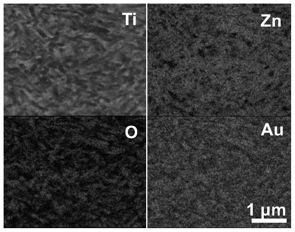
[0106] The surface of the sample treated in Example 1 was analyzed for elemental content. Energy Spectrum ( Figure 1b ) shows that zinc, oxygen, gold, and titanium elements are evenly distributed on the surface of the sample, indicating that the zinc oxide coating and gold nanoparticles are evenly distributed.


PUM


Abstract

The invention relates to an antimicrobial semiconductor coating layer with a detection effect and a preparation method and application thereof, and particularly discloses an antimicrobial semiconductor coating layer capable of self-detecting the number of microorganisms, and the semiconductor coating layer is a semiconductor nano array generated in situ on an epoxy group generated on a substrate, and the semiconductor nano array is selected from a zinc oxide nano material array, a titanium dioxide nano material array and a silicon array; and the surface of the semiconductor nano array further comprises modification of metal nano particles. The invention also discloses an application of the semiconductor coating layer. The semiconductor coating layer provides the antimicrobial activity of the substrate and can detect the microbial content of the surface of the substrate at the same time. The antimicrobial semiconductor coating layer integrates the functions of monitoring bacteria and resisting bacteria, and can monitor the infection condition in real time in the anti-infection process and prompt a user to take corresponding measures in time.

Description

technical field [0001] The invention belongs to the field of biological detection, and in particular relates to a semiconductor coating with anti-microbial and detection effects and its application in anti-microbial and detection of microbial content. Background technique [0002] Implant surgery is one of the common clinical treatment options to improve the quality of life of patients, but a key factor leading to the failure of implant surgery is bacterial infection. Appropriate modification of the implant surface can achieve an antibacterial surface and effectively reduce the infection rate. At the same time, if the antibacterial interface can realize real-time monitoring of the number of bacteria, it will bring great convenience to doctors in timely monitoring of patient infection. [0003] Electron transfer is a common physical phenomenon that occurs at an interface with a potential difference. Studies have shown that electron transfer between materials and bacteria play...

Claims


Application Information

Patent Timeline
Patent Type & Authority Applications(China)
IPC IPC(8): G01N15/10A61L31/08A61L31/14A61L31/16C23C14/18C23C14/35B82Y40/00B82Y15/00
CPCG01N15/1031A61L31/088A61L31/14A61L31/16C23C14/185C23C14/35B82Y40/00B82Y15/00G01N2015/1006A61L2300/102A61L2300/404A61L2300/606A61L2400/18A61L2420/02
Inventor 王国敏唐楷为孟哲一王怀雨朱剑豪
Owner SHENZHEN INST OF ADVANCED TECH
Why Eureka
Try Eureka