Method for making modular spot converting distributed-feedback Prague laser by using quantum trap confounding

A quantum well hybrid and mode-spot converter technology, which is applied in the direction of lasers, phonon exciters, laser components, etc., can solve the problems of small process tolerance, increased radiation loss, and low reliability of devices, so as to reduce crystal growth the number of times, reduce the effect of Auger complex, and reduce the number of growth

Inactive Publication Date: 2007-02-07
INST OF SEMICONDUCTORS - CHINESE ACAD OF SCI
View PDF0 Cites 3 Cited by
  • Summary
  • Abstract
  • Description
  • Claims
  • Application Information

AI Technical Summary

Problems solved by technology

[0011] 1) The laser adopts a buried structure, the number of epitaxy increases, the process is complicated, and the reliability of the device is low
[0012] 2) The mold spot converter adopts vertical wedge shape, adopts butt-joint (that is, docking) epitaxy technology or gradual corrosion and other processes, it is not easy to obtain good secondary growth crystal quality; and the interface treatment is very difficult, and it is easy to appear multi-mode at the interface , resulting in deterioration of mode characteristics, increased radiation loss, poor repeatability of device fabrication, and small process tolerance
[0013] 3) Although some lasers and mode-spot converters use ridge-type double-waveguide structures, the InP space layer in the middle is as thick as 2 μm, and the device cost is high
[0014] 4) Some use the alternate growth of InP and InGaAsP for the lower waveguide in the double waveguide structure to obtain the effective refractive index they need. Obviously, this structure is extremely complicated

Method used


Image

  • Method for making modular spot converting distributed-feedback Prague laser by using quantum trap confounding
  • Method for making modular spot converting distributed-feedback Prague laser by using quantum trap confounding
  • Method for making modular spot converting distributed-feedback Prague laser by using quantum trap confounding

Examples


Embodiment

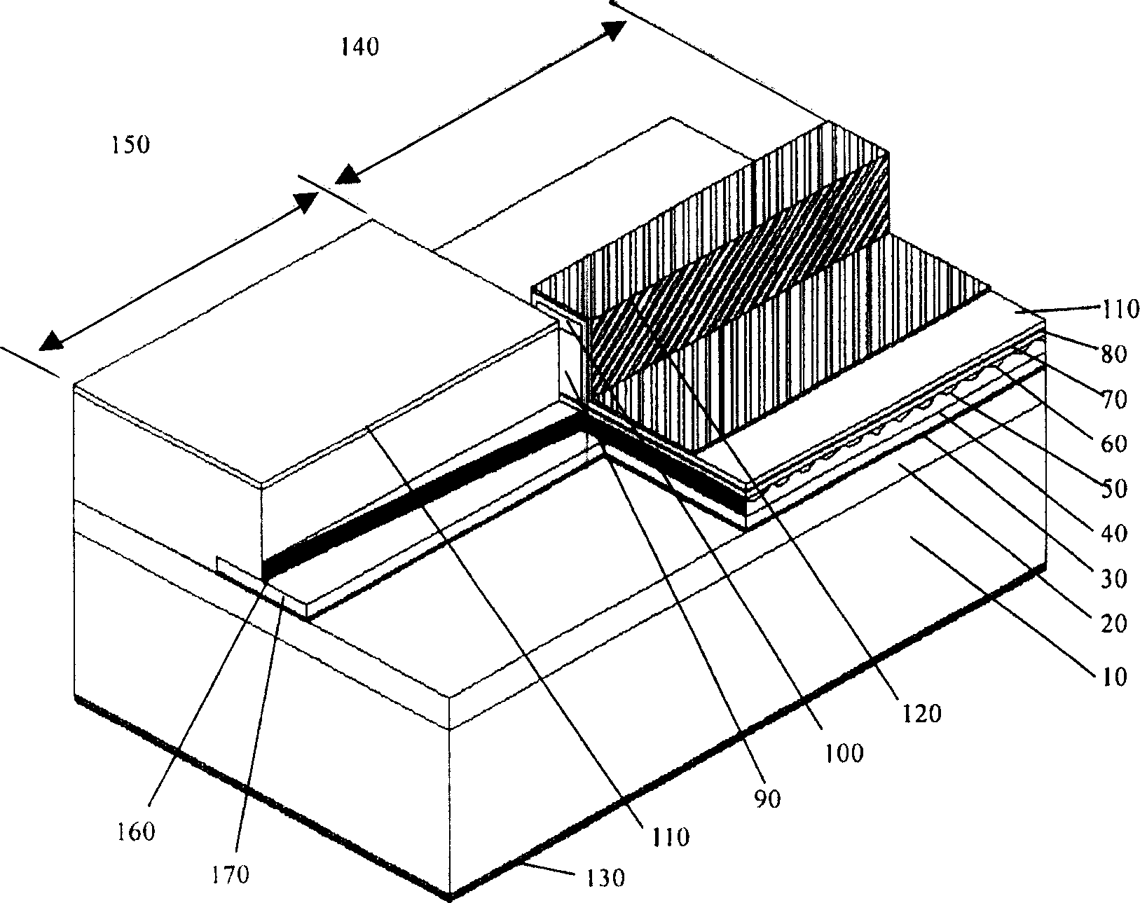
[0074] see again figure 1 , the present invention uses quantum well hybridization as a method for mode spot conversion distributed feedback Bragg laser, characterized in that it comprises the following manufacturing steps:

[0075] (1), the 2-inch n-InP substrate undergoes strict decontamination (heating and boiling with ethanol, trichlorethylene, lactone, and ethanol in sequence) → pickling (soaking in concentrated sulfuric acid for 1 to 2 minutes) → water washing (deionization Rinse with water for more than 50 times) → throw it after treatment, put it into the growth chamber, the growth temperature is 655°C, the growth pressure is 22mbar, and the graphite boat rotates at 75-80 rpm. Growth rate 0.4~0.7nm / s;

[0076] (2) On the surface of n-type indium phosphide substrate (100), epitaxially grow n-type indium phosphide buffer layer (0.5 μm thick), lower waveguide layer (thickness 50 nm, bandgap wavelength 1.1 μm), 0.2 μm phosphorus Indium space layer, lower optical confineme...


PUM


Abstract

The invention relates to a method for using quantum well mixing to produce mode speckle conversion distributed feedback Bragg lasers, which comprises: growing n-type indium phosphate buffer layer on the substrate; using silica dioxide to mask the distributed feedback Bragg lasers, and generating point corrosion on the characteristic indium phosphate pour buffer layer at the mode speckle converter; corroding the silica dioxide protective layer; heating chip, keeping warm and annealing; corroding the protective layer; grating the whole chip; corroding the characteristic indium phosphate pour buffer layer; etching the upper and lower ridge pilot structures on the converter; cleaning the chip; growing p-type indium phosphate layer, indium gallium arsenic phosphate etching stopping layer, p-type indium phosphate package and high-doping p-type indium gallium arsenic ohm electrode contact layer; growing silica dioxide insulated layer on the whose chip; opening electrode window at the laser, and splashing p electrode; extending the substrate; boiling n electrode at the back; slicing the sample into tubular core.

Description

technical field [0001] The invention relates to the use of quantum well hybrid and asymmetric double waveguide technology, and the common wet etching and photolithography process to manufacture a monolithic integrated semiconductor distributed feedback (DFB) laser and a mode spot converter. Background technique [0002] The output spot of the semiconductor laser (LD) used in the optical fiber communication system is small (less than 2 μm in diameter) and has an elliptical shape; while the intrinsic spot of the glass single-mode fiber connected to the semiconductor laser is relatively large (about 8-10 μm in diameter) , in a symmetrical round shape. The difference in the size and shape of the eigenmode field between the laser and the single-mode fiber leads to a large mode mismatch between the two, low coupling efficiency, and small offset tolerance. In order to couple the elliptical spot output by the semiconductor laser to the optical fiber with high quality and high effic...

Claims


Application Information

Patent Timeline
Patent Type & Authority Applications(China)
IPC IPC(8): H01S5/00H01S5/20H01S5/343
Inventor 侯廉平王圩朱洪亮
Owner INST OF SEMICONDUCTORS - CHINESE ACAD OF SCI
Why Eureka
Try Eureka