
Patterned Si substrate-based LED epitaxial wafer and preparation method therefor

a substrate-based, led-based technology, applied in the field of led epitaxy, can solve the problems of difficult preparation, restricted development of high-power leds using sapphire substrates, and difficult heat dissipation, so as to achieve effective protection, avoid melt-back reaction, and high quality

Active Publication Date: 2021-03-30
ENKRIS SEMICON
View PDF16 Cites 0 Cited by
  • Summary
  • Abstract
  • Description
  • Claims
  • Application Information

AI Technical Summary

Benefits of technology

The present invention provides a way to prepare high-quality LED materials and devices on patterned silicon substrates. By using Al2O3 coatings on patterned Si substrates and growing an AlN nucleation layer first, followed by a GaN epitaxial layer, the problem of AlN growth on the substrate is avoided, and a flat GaN single crystal epitaxial film can be formed. Additionally, the use of patterned Si substrates with a rough surface pattern allows for easier pattern transfer and reduces the difficulty of back surface roughening. Another advantage of patterned Si substrates is that the dislocation density of the epitaxial material is reduced, improving LED performance. Adding a stress buffer layer to the entire LED device structure also helps prevent surface cracking caused by a tensile stress. Overall, the invention provides a more efficient and cost-effective way to produce high-quality LED devices.

Problems solved by technology

In the past 20 years, researchers have continuously explored and improved the GaN epitaxial growth technology, but it is difficult to prepare the GaN bulk material which is the most ideal homogenous substrate for growing GaN epitaxial layer (because GaN has a high melting point (2800° C.) and equilibrium vapor pressure (4.5 GPa) is large); therefore, epitaxial growth of GaN is mostly performed on a heterogeneous substrate.
However, the sapphire has a low thermal conductivity so that making it difficult to dissipate heat, which also seriously restricts the development of high-power LEDs using sapphire substrates.
SiC substrate has excellent thermal conductivity (4.49 W / cm·K), and its lattice mismatch with GaN is only 3.5%, however due to its high price and small substrate size, it is difficult to reduce the cost, and can only be used in high-end applications.
However, the main problem with epitaxially growing GaN on a Si substrate is the presence of large stress in the GaN-on-Si epitaxial film, which causes surface cracking problems.
In addition, when a GaN epitaxial material is grown on a Si substrate, if not treated, the Si substrate may react with Ga atoms in the atmosphere of ammonia (NH3) (referred to as a “melt-back reaction”), causing a large amount of surface defects, unable to produce the device.
Surface roughening on N surfaces of AlN nucleation layers can be carried out by a dry or wet process, but each of the fabrication process is relatively difficult, the rate of dry etching for AlN is slow, and wet etching requires a higher temperature.
When AlN is deposited on a Si substrate, it can be attached to various directions of the patterned Si substrate, and it is impossible to prepare a single crystal GaN epitaxial material.

Method used


Image

  • Patterned Si substrate-based LED epitaxial wafer and preparation method therefor
  • Patterned Si substrate-based LED epitaxial wafer and preparation method therefor
  • Patterned Si substrate-based LED epitaxial wafer and preparation method therefor

Examples


Embodiment Construction

[0042]The invention will be described in detail below in conjunction with the specific embodiments shown in the drawings. However, the embodiments are not intended to limit the invention, and the structures, methods, or functional changes made by those skilled in the art in accordance with the embodiments are included in the scope of the present invention.

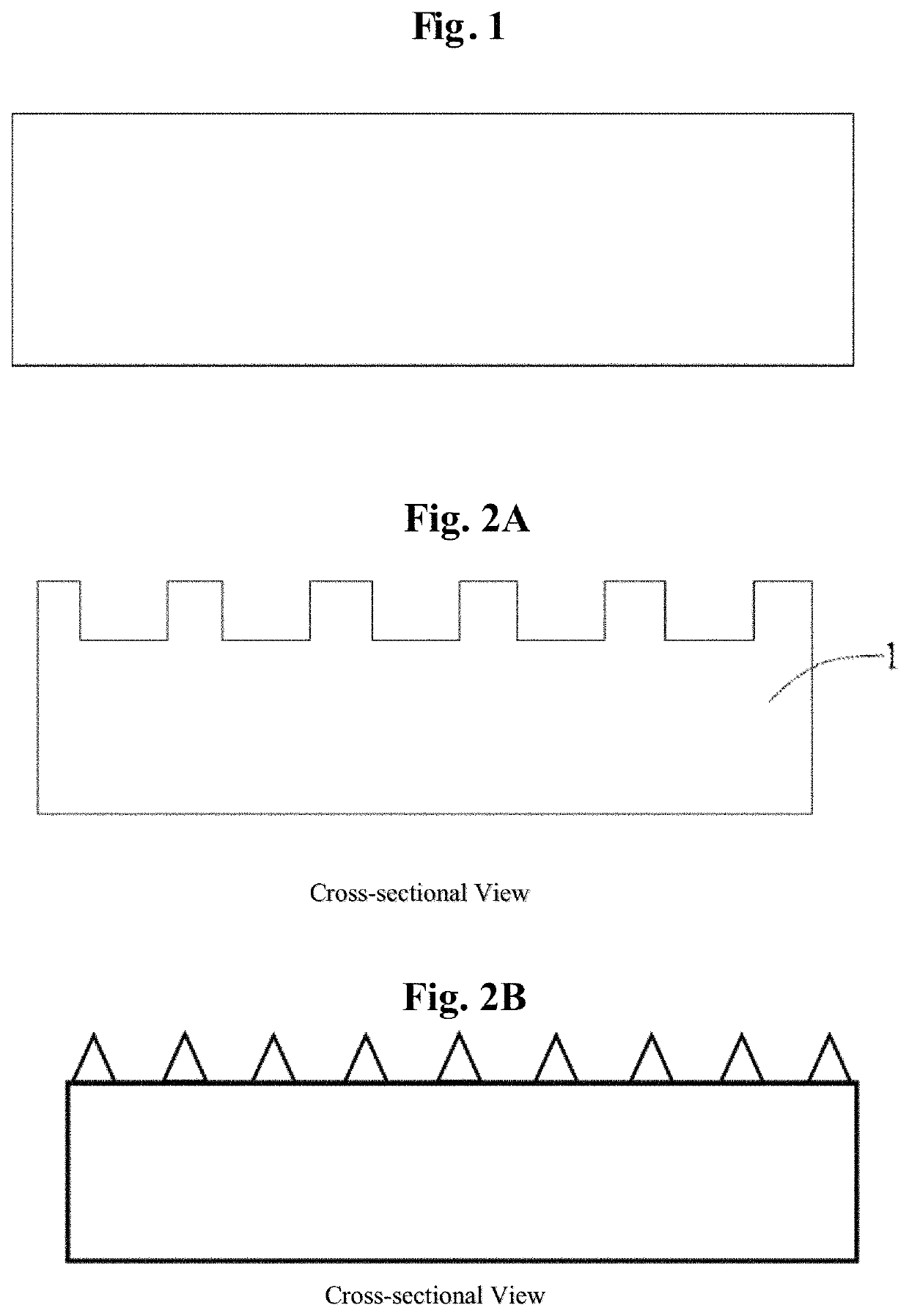
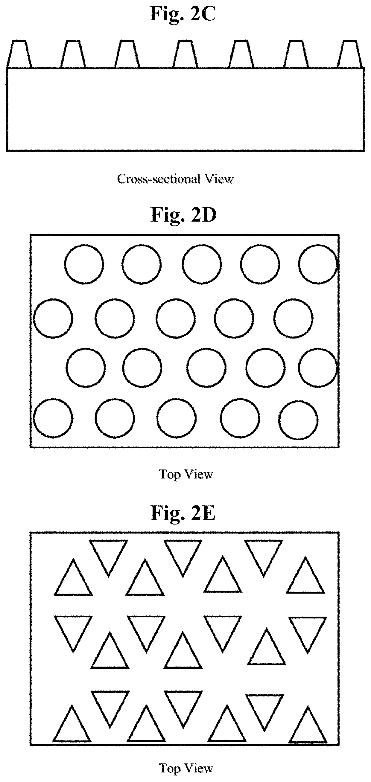
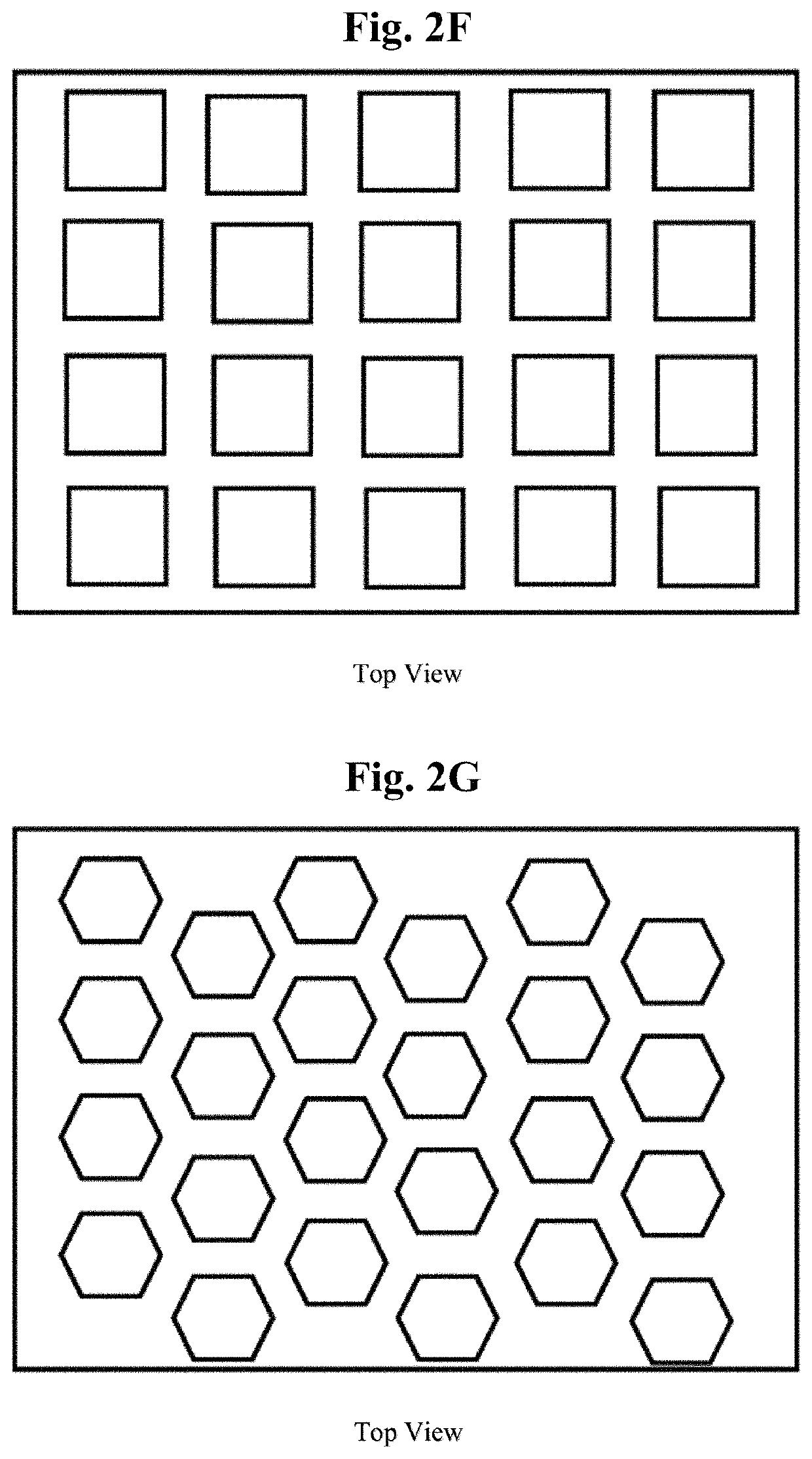
[0043]Referring to FIG. 1 to FIG. 11, the method for preparing a patterned Si substrate-based LED epitaxial wafer in the embodiment specifically includes the following steps:

[0044](1) Preparing a flat Si substrate (as shown in FIG. 1), first etching a patterned structure on a flat Si substrate (shown in FIG. 1) to prepare a patterned silicon substrate (PSS) 1. Preferably, the present invention can optionally etch the patterned structure by dry etching.

[0045]The Si substrate is a Si (111) crystal face or a Si (100) crystal face or a Si (110) crystal face, and the doping type is n-type or p-type.

[0046]In the present invention, the pa...


PUM

PropertyMeasurementUnit
melting pointaaaaaaaaaa
thermal conductivityaaaaaaaaaa
thicknessaaaaaaaaaa

Abstract

An patterned Si substrate-based LED epitaxial wafer and a preparation method therefor, the LED epitaxial wafer comprising: a patterned Si substrate (1) and an Al2O3 coating (2) growing on the patterned Si substrate (1); sequentially growing on the Al2O3 coating (2) are a nucleating layer (3), a first buffer layer (4), a first insertion layer (5), a second buffer layer (6), a second insertion layer (7), an n-GaN layer (8), a quantum well layer (9), a p-GaN layer (10), an n-electrode (14) electrically connected to the n-GaN layer and a p-electrode (13) electrically connected to the p-GaN layer. The present invention is suitable for the preparation of large-sized LED epitaxial wafers. Furthermore, the crystal quality is improved, and the light extraction efficiency of the LED die is improved.

Description

[0001]The present application claims priority to Chinese Patent Application No. CN201610187818.8, entitled “PATTERNED SI SUBSTRATE-BASED LED EPITAXIAL WAFER AND PREPARATION METHOD THEREFOR”, filed on Mar. 29, 2016, all of which is incorporated herein by reference.FIELD OF THE INVENTION[0002]The invention relates to the field of LED epitaxy and particularly relates to a patterned Si substrate-based LED epitaxial wafer and preparation method therefor.BACKGROUND OF THE INVENTION[0003]Band gap of GaN-based III-V compound semiconductor materials (AlN, GaN, InN, and ternary or quaternary alloy materials composed of them) can be continuously adjustable from 0.7 eV to 6.2 eV at room temperature, and the color covers the entire visible light band and a part of infrared, ultraviolet band, which has a wide range of applications and developments in optoelectronic devices such as lasers (LDs), light-emitting diodes (LEDs), full-spectrum solar cells and detectors. In 1989, Akasaki and Amono succe...

Claims


Application Information

Patent Timeline
Patent Type & Authority Patents(United States)
IPC IPC(8): H01L33/12H01L33/44H01L33/00H01L33/22H01L33/18H01L33/02H01L33/20
CPCH01L33/12H01L33/007H01L33/0075H01L33/18H01L33/22H01L33/44H01L33/025H01L33/20H01L2933/0025H01L33/16
Inventor ZHANG, LIYANGCHENG, KAI
Owner ENKRIS SEMICON
Learn More