Clathrate compounds, manufacture thereof, and thermoelectric materials, thermoelectric modules, semiconductor materials and hard materials based thereon

a technology of clathrate compounds and clathrate compounds, which is applied in the direction of non-metal conductors, conductors, energy input, etc., can solve the problems of limited to certain, poor thermoelectric conversion efficiency of conventional thermoelectric materials, and is problematic to propose the use of thermoelectric materials, etc., to achieve excellent applicability, favourable thermal conductivity, electrical conductivity and semiconductor like properties

Inactive Publication Date: 2003-10-23
IHI CORP +1
View PDF2 Cites 22 Cited by
  • Summary
  • Abstract
  • Description
  • Claims
  • Application Information

AI Technical Summary

Benefits of technology

0050] The effects of the present invention are as described below.
0051] A clathrate compound according to the present invention has properties resembling those of a metal, displaying favourable thermal conductivity, electrical conductivity and semiconductor like properties, and also possessing a high level of hardness.
0052] A clathrate compound according to the present invention displays excellent applicability as a thermoelectric material, a semiconductor material, or a hard material.
0053] Furthermore, with a method of manufacturing a clathrate compound according to the present invention, a superior clathrate compound which has properties resembling tho...

Problems solved by technology

For example, various methods for Using thermoelectric materials are under investigation, but conventional thermoelectric materials display poor thermoelectric conversion efficiency, and are limited to certain uses where reliability is not particularly important.
Consequently, it has been deemed problematic to propose the use of thermoelectric materials for typical uses such as-waste heat power generation.
Because the temperature range for stable operation of this type of compound semiconductors is low, and ensuring good heat dissipation is a large problem, the development of the semiconductors which will also operate at higher temperatures has been greatly needed.
Although cubic boron nitride (CBN) is able to be synthesized, it remains limited to applications such as abrasive grits, and a material which can be used for members in mechanical components and sliding components which require low friction and good abrasion resistance has been keenly sought.
For example in the case of metals, although offering the benefits of a large electrical conductivity, they suffer from having a large thermal conductivity and a small Seebeck coefficient.
In the case of semiconductors, although offering the advantages of a small thermal conductivity and a large Seebeck coefficient, because the electrical conductivity is small, they can not be considered a high efficiency thermoelectric materials.
However, the efficiency thereof at 100.degree. C. or higher is low, and it is unable to withstand practical use.
In contrast, with conventional semiconductor materials, the temperature range for stable operation is low, meaning the operating environment is limited to a thermal environment close to room temperature.
For example, widely used silicon devices typically have a stable operating temperature range below 125.degree. C., and so electronic equipment utiliz...

Method used


Image

  • Clathrate compounds, manufacture thereof, and thermoelectric materials, thermoelectric modules, semiconductor materials and hard materials based thereon
  • Clathrate compounds, manufacture thereof, and thermoelectric materials, thermoelectric modules, semiconductor materials and hard materials based thereon
  • Clathrate compounds, manufacture thereof, and thermoelectric materials, thermoelectric modules, semiconductor materials and hard materials based thereon

Examples


example 1

[0239] Powders of Ba, Si and Al were weighed and combined to produce a Ba:Si:Al constituent ratio (atom %) of 8:26:20, and a powdered mixture then prepared by mechanical alloying treatment. The powdered mixture was submitted to preliminary heating at 800.degree. C. under an atmosphere of Ar gas for a period of 24 hours, and following this preliminary heating, was then re-ground to an average granular diameter of 100 .mu.l, before undergoing plasma sintering in a plasma sintering apparatus at a temperature of 850.degree. C. and a pressure of 40 MPa for a period of 30 minutes.

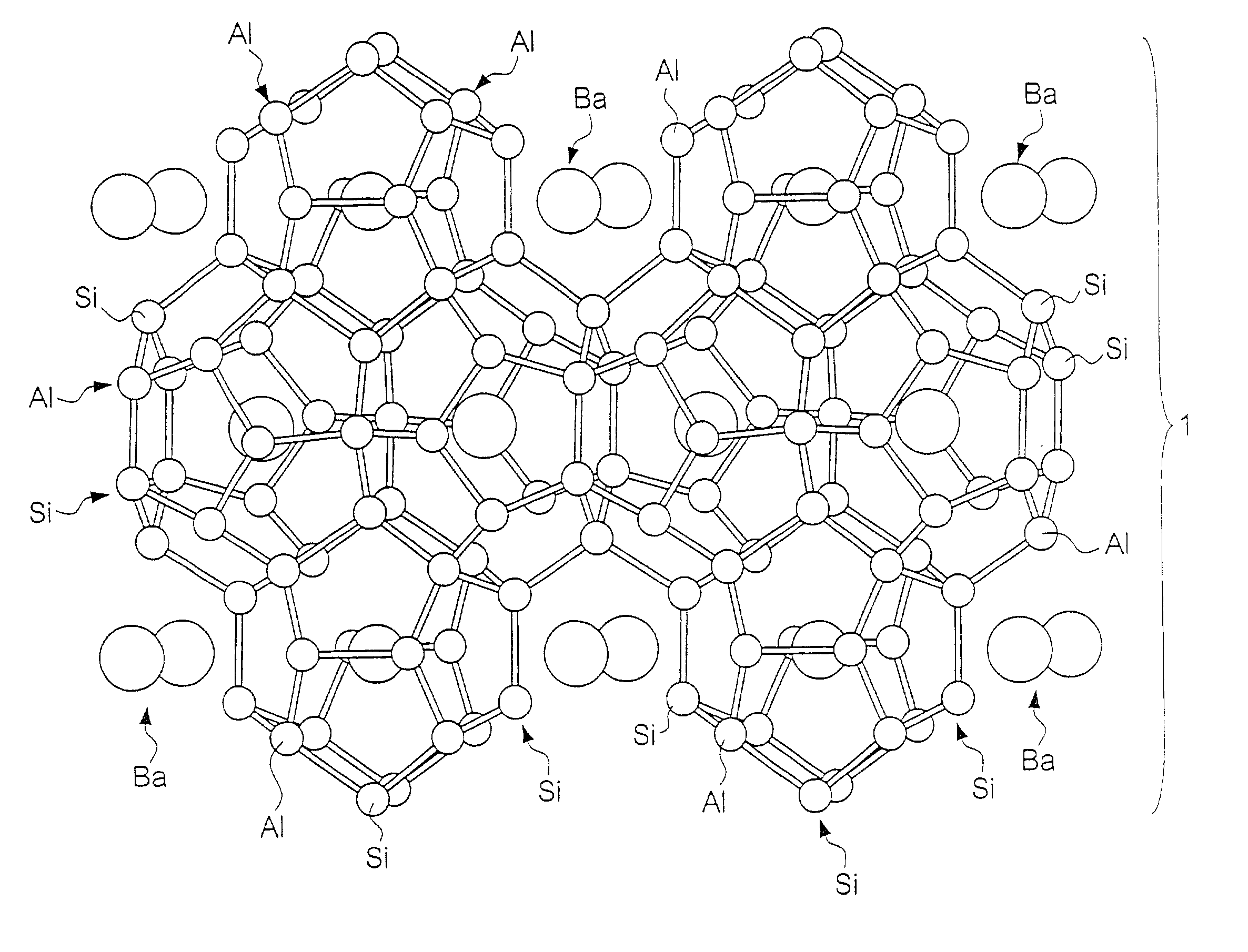
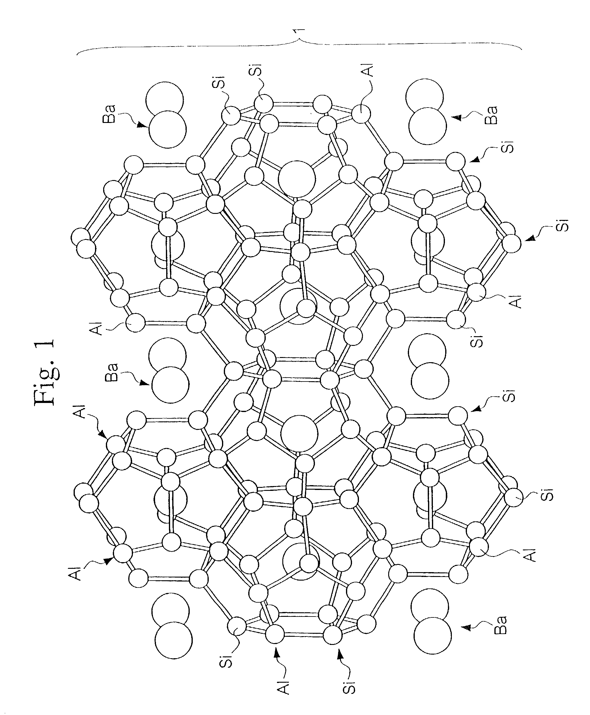
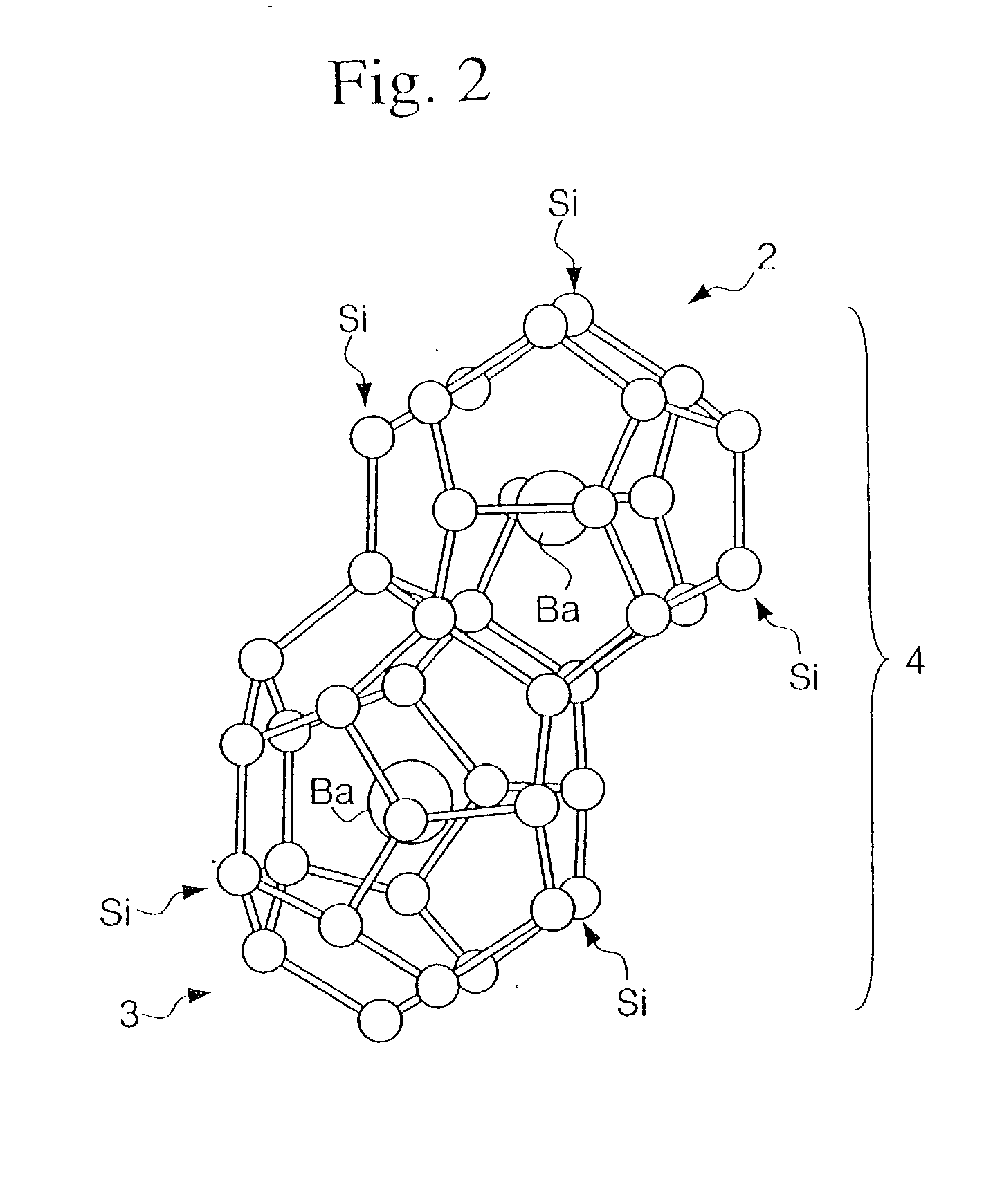
[0240] X-ray analysis of the sintered product confirmed a silicon clathrate 46 Ba.sub.8@(Si.sub.26,Al.sub.20) structure in the space group Pm3m, origin at 4 3 m (note that normally in crystallographic analyses the "3" of Plm3m is displayed with an overline, but there the overline is represented by 3), and with a lattice constant of 10.3 .ANG.. Furthermore, a measurement of the figure of merit (ZT) of the sintered...

example 2

[0241] Powders of Ba, Si and P were weighed and combined to produce a Ba:Si:P constituent ratio (atom %) of 8:26:20, and a powdered mixture then prepared by mechanical alloying treatment. The powdered mixture was submitted to preliminary heating at 800.degree. C. under an atmosphere of Ar gas for a period of 24 hours, and following this preliminary heating, was then re-ground to an average granular diameter of 100 .mu.m, before undergoing plasma sintering in a plasma sintering apparatus at a temperature of 850.degree. C. and a pressure of 40 MPa for a period of 30 minutes.

[0242] X-ray analysis of the sintered product confirmed a silicon clathrate 46 Ba8@(Si.sub.26,P.sub.20) structure in the space group Pm3m, origin at 4 3 m (note that normally in crystallographic analyses the "3" of Pm3m is displayed with an overline, but here the overline is represented by 3), and with a lattice constant of 10.5 .ANG.. Furthermore, a measurement of the figure of merit (ZT) of the sintered product a...

example 3

[0244] Calcium carbide (CaC.sub.2) was melted by heating at up to 2,500.degree. C., and following solidification was insulated inside a furnace and cooled gradually to 1,000.degree. C. The furnace was then maintained at a temperature of 1,000.+-.10.degree. C. for a period of 120 hours (5 days). The resulting ingot was ground finely and washed with water. Following drying, the powder was inserted into a pressure sintering apparatus and sintered for 20 hours at 1000.degree. C. and 100 MPa. Structural analysis of the crystals obtained, by X-ray diffraction, revealed a lattice constant of 0.68 nm, and the diffraction peaks confirmed the encapsulation of Ca atoms within clusters of 20 carbon atoms and clusters of 24 carbon atoms. Composition analysis by EPMA showed a Ca:C atomic weight ratio of 7.62:45.62 as opposed to the target Ca:C ratio of 8:46. Furthermore the results of a hardness test revealed a hardness equivalent to cubic boron nitride. Moreover, confirmation or the current dire...


PUM


Abstract

In high-tech fields such as electronics, the development of new high performance materials which differ from conventional materials has received much attention. An object of the present invention is to provide a clathrate compound which can be used as a thermoelectric material, a hard material, or a semiconductor material. Atoms of an element from group 4B of the periodic table are formed into a clathrate lattice, and a clathrate compound is then formed in which specified doping atoms are encapsulated within the clathrate lattice, and a portion of the atoms of the clathrate lattice are substituted with specified substitution atoms. Suitable doping atoms are atoms from group 1A, group 2A, group 3A, group 1B, group 2B, group 3B, group 4A, group 5A, group 6A, and group 8, and suitable substitution atoms are atoms from group 1A, group 2A, group 3A, group 1B, group 2B, group 3B, group 5A, group 6A, group 7A, group 5B, group 6B, group 7B, and group 8 of the periodic table. Suitable manufacturing methods include melt methods and sintering methods, and moreover intercalant intercalation compounds or the like may also be used as raw materials.

Description

BACKGROUND OF TTE INVENTION[0001] 1. Field of the Invention[0002] The present invention relates to clathrate compounds, high efficiency thermoelectric materials and thermoelectric modules utilizing the clathrate compound, the semiconductor materials or hard materials utilizing the clathrate compounds, as well as manufacturing methods thereof.[0003] 2. Description of the Related Art[0004] Recently, in high-tech fields such as electronics, the development of new high performance materials which differ greatly from conventional materials has received much attention.[0005] For example, various methods for Using thermoelectric materials are under investigation, but conventional thermoelectric materials display poor thermoelectric conversion efficiency, and are limited to certain uses where reliability is not particularly important. Consequently, it has been deemed problematic to propose the use of thermoelectric materials for typical uses such as-waste heat power generation.[0006] Furthe...

Claims


Application Information

Patent Timeline
IPC IPC(8): C01B33/06H01L35/14
CPCH01L35/14C01B33/06Y02P20/129H10N10/851
Inventor EGUCHI, HARUKISUZUKI, AKIHIKOTAKAHASHI, SATOSHIMIYAHARA, KAORUTANAKA, TOHRUKIHARA, SHIGEMITSUTSUMURAYA, KAZUO
Owner IHI CORP
Why Eureka
Try Eureka