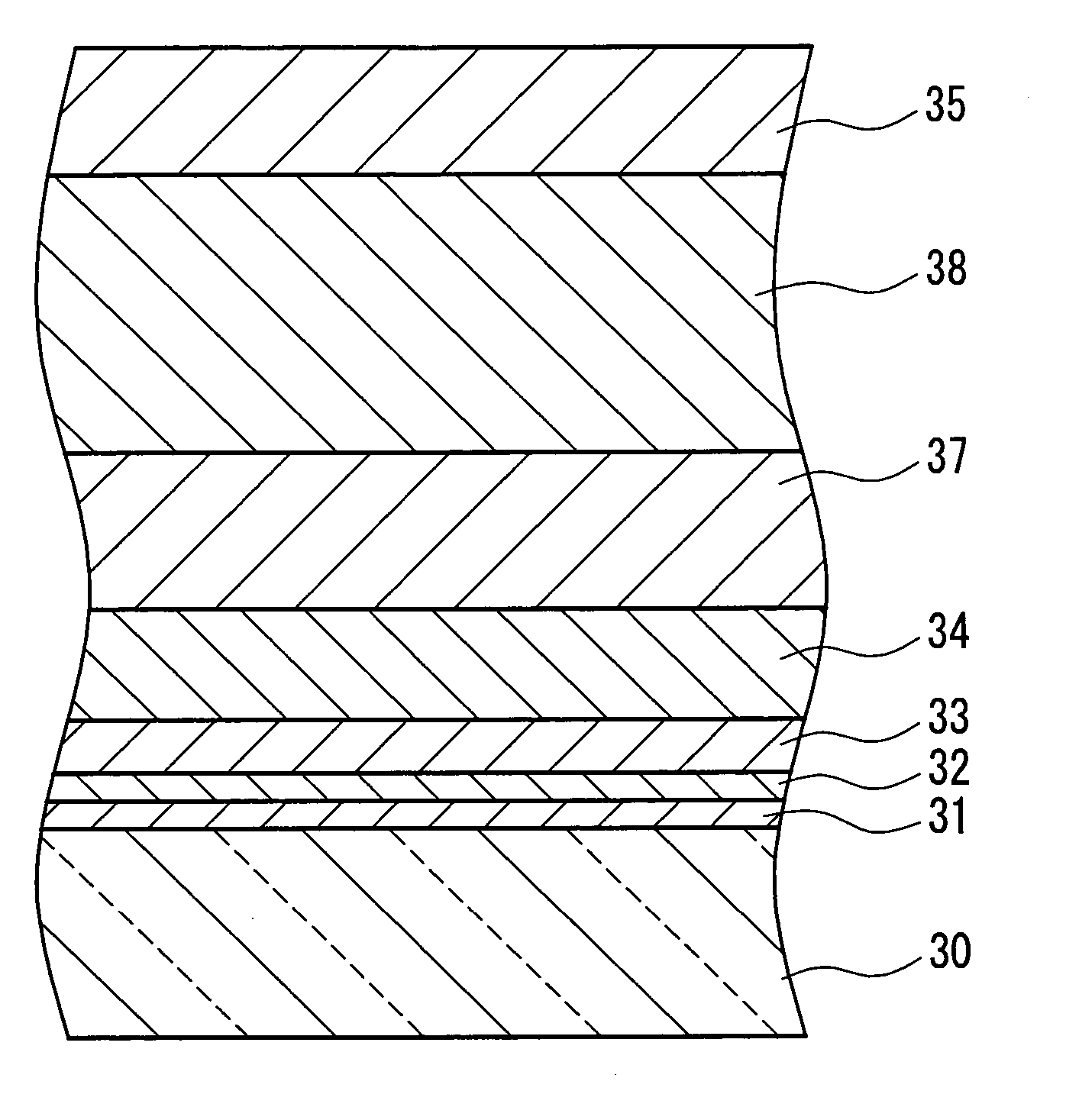
Method for forming thin film, substrate having transparent electroconductive film and photoelectric conversion device using the substrate

a technology of electroconductive film and substrate, which is applied in the direction of coating, chemical vapor deposition coating, semiconductor devices, etc., can solve the problems of difficult to obtain a uniform film thickness, low thermal deposition rate of thin film containing metal oxide, and inability to achieve uniform film thickness, etc., to achieve low reactivity and low deposition rate

Active Publication Date: 2005-06-09
NIPPON SHEET GLASS CO LTD
View PDF11 Cites 18 Cited by
  • Summary
  • Abstract
  • Description
  • Claims
  • Application Information

AI Technical Summary

Benefits of technology

[0041] The method for forming the metal-containing thin film is not particularly limited as long as it is a thermal decomposition method, and examples include a CVD method and a solution-spraying method in which a solution material is sprayed onto a heated substrate. If the metal-containing thin film and the thin film containing a crystalline metal oxide as the main component are formed by the same formation method, they can be formed within a short time through a series of manufacturing steps; for this reason, it is preferable that these be formed by the same method in terms of industrial production efficiency.
[0042] Because the metal-containing thin film needs to function as starting points for crystal growth in the thin film containing a crystalline metal oxide as the main component, it is necessary that the film be formed uniformly on the surface of the substrate or of the undercoating film, desirably with bumps at constant intervals on the surface. For that reason, the film deposition rate for the metal-containing thin film is slower than the film deposition rate for the thin film containing a crystalline metal oxide as the main component. Specifically, the film deposition rate should preferably be 20 to 2500 nm / min. Nevertheless, in the case of the film deposition rate exceeding 600 nm / min., it is preferable that the surface of the undercoating film (second undercoating layer) be provided with bumps and depressions. Even if the film deposition rate for the metal-containing thin film itself is slow, the thickness thereof is 250 nm or less, as will be described later, and significantly thinner than that of the thin film containing a crystalline metal oxide as the main component (transparent conductive film); therefore, the film deposition rate as a whole, which includes that for the thin film containing a crystalline metal oxide as the main component, is not degraded considerably. Rather, because of the presence of the metal-containing thin film, the film deposition rate for the thin film containing a crystalline metal oxide as the main component can be made faster; therefore, if the metal-containing thin film is formed to be relatively thin and in addition the thin film containing a crystalline metal oxide as the main component is formed more quickly at a higher temperature, the film deposition rate as a whole can be made faster.
[0043] Examples of the means to make the film deposition rate for the metal-containing thin film slower than the film deposition rate for the thin film containing a crystalline metal oxide as the main component include a means in which the surface temperature of the substrate or the undercoating film is set to be fairly low in forming the metal-containing thin film and thereafter, after reheating, the thin film containing a crystalline metal oxide as the main component is formed, and a means in which a raw material with low reactivity is used. Nevertheless, in cases where, the undercoating film, the metal-containing thin film, and the thin film containing a crystalline metal oxide as the main component are formed successively on a glass ribbon in a float process by a CVD method, the temperature of reaction system during the formation of the metal-containing thin film form becomes higher than the temperature of reaction system during the deposition of the thin film containing a crystalline metal oxide as the main component. In this case, it is conceivable to reheat the glass ribbon using a burner or the like after the formation of the metal-containing thin film in order to make the temperature of reaction system for the thin film containing a crystalline metal oxide as the main component higher, but by doing so, temperature unevenness may occur in the glass ribbon, leading to the risk of degrading the formability of glass. In view of this case, it is desirable to reduce reactivity by varying the types of raw materials, or to lower the film deposition rate by reducing the thickness of the metal-containing thin film. For the chloride of a metal, those which do not contain organic substances, such as tin dichloride, tin tetrachloride, titanium chloride, zinc chloride, and indium chloride, are suitable for the purpose of reducing the environmental load.
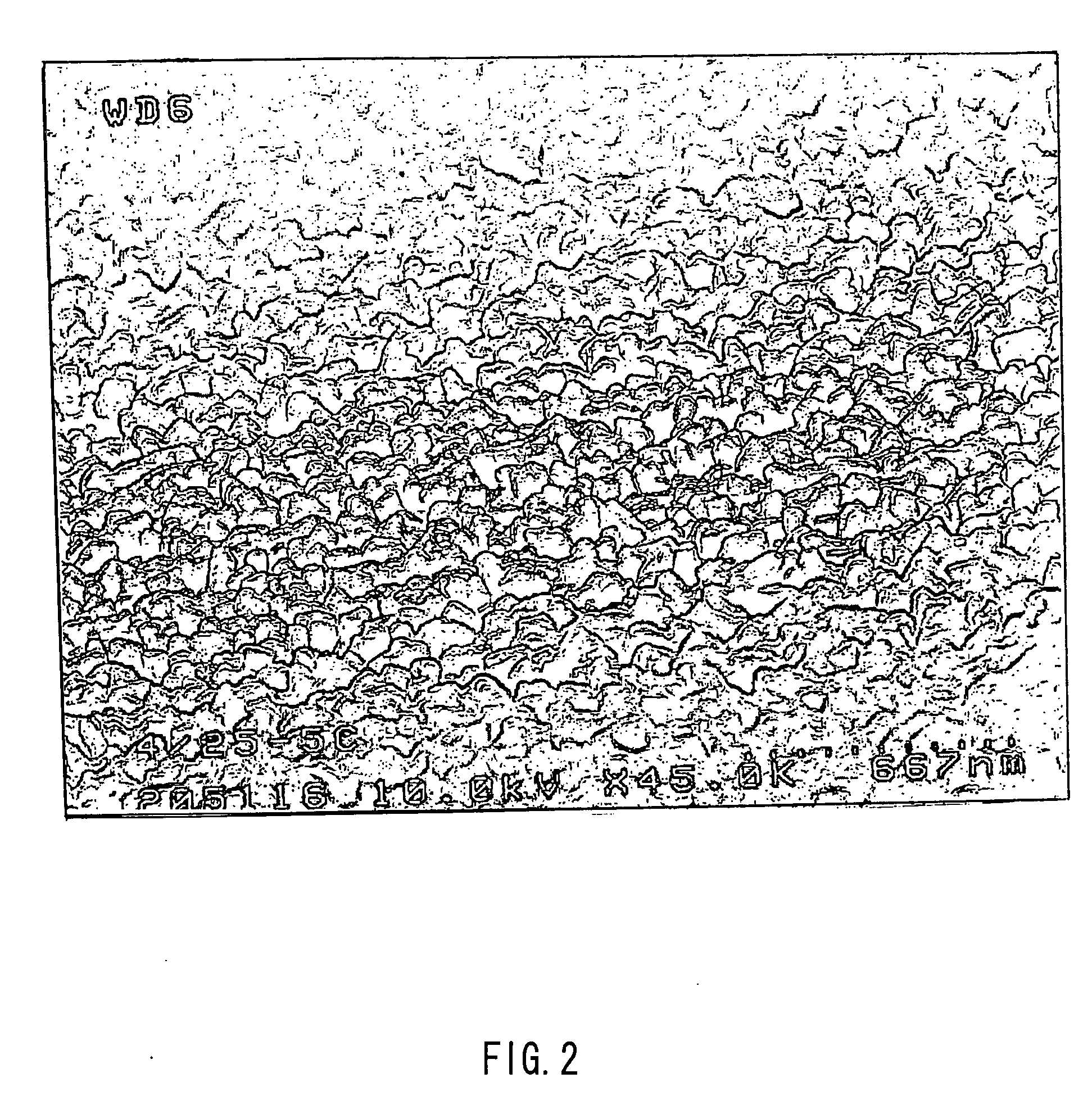
[0044] The metal-containing thin films may be those including metal-containing particles, or those that contain a metal as its compositional component. For example, when a metal-containing thin film that has a crystalline metal oxide such as tin oxide or titanium oxide as the main component is formed by a CVD method, bumps that can be clearly distinguished from the other portion may be formed on the thin film in some cases, but in other cases, very small bumps and depressions are formed on the surface and the vertices of those bumps and depressions need to be interpreted as the bumps. In other words, a surface shape of a metal-containing thin film may not be determined easily if it is part of surface roughness or can be considered as a bump. In this invention, it is sufficient that the metal-containing thin film functions as starting points for crystal growth, and even if it cannot be distinguished clearly whether a shape forms a vertex of the surface roughness or a bump, that is not a problem per se as long as the foregoing function is fulfilled. Additionally, even if the metal-containing thin film does not have clearly-distinguishable bumps formed on the surface thereof, the function as the starting points for crystal growth can be fulfilled when crystal growth can be induced in the thin film containing a crystalline metal oxide as the main component.
[0045] For reference, it has been confirmed that in the case of forming the metal-containing thin film by a CVD method, white turbidity is not produced in the thin film containing a crystalline metal oxide as the main component even with increased film deposition rates for the metal-containing thin film and increased film thicknesses when the concentration of a metal-containing gas in the mixed gas, which serves as the raw material therefor, is lowered. This seems to be because the lowering of the concentration of the metal-containing gas suppresses abrupt crystal growth that originates from the high concentration metal-containing gas residing locally.
[0046] The metal-containing thin film should preferably be in a condition such that the thickness is 10 to 250 nm, and the surface thereof has a multiplicity of bumps formed thereon and having a height of 10 to 200 nm. When the thickness is less than 10 nm, there is a risk of the undercoating film being not completely covered; on the other hand, when exceeding 250 nm, the bumps become too large and too high, the risk of generating giant crystal grains in the thin film containing a crystalline metal oxide as the main component increases. The more preferable thickness of the metal-containing thin film is 30 to 200 nm.

Problems solved by technology

Since a glass sheet provided with this thin film reduces the total solar energy transmittance and does not allow the heat within rooms to escape to the outdoors, it is widely available in the market as a low-emissivity glass.
Such methods of forming a thin film containing a metal oxide that utilize thermal decomposition methods are inferior to physical vapor deposition methods, such as a sputtering method, in that it is difficult to obtain a uniform film thickness; nevertheless, they are capable of forming a thin film over a wide area within a short time at a relatively uniform thickness and therefore are suitable for mass production of industrial products.
Moreover, crystals become more difficult to grow, slowing down the film deposition rate.
However, since an undercoating film made of silicon oxide has a very smooth surface, it is obvious that when a thin film made of tin oxide is deposited at a film deposition rate of as fast as 6234 nm / min. without performing any treatment thereto, giant crystal grains should form, causing a white turbidity.
There has been a problem that if a photoelectric conversion device is constructed by an amorphous silicon layer formed on this transparent conductive film, the amorphous silicon film, which serves as the photoelectric conversion layer, is not uniformly formed, and the efficiency of the solar cell is reduced.
Furthermore, there has been a problem when dimethyltin dichloride or monobutyltin trichloride is used as tin materials other than those described above, in that although the white turbidity does not occur, the absorptance becomes large in the wavelength range of 400 to 700 nm, in which the light quantity of solar light spectrum reaching the Earth's ground is large, particularly in the short wavelength range thereof, and as a result, the incident light volume on the photoelectric conversion layer in the solar cell is small.

Method used


Image

  • Method for forming thin film, substrate having transparent electroconductive film and photoelectric conversion device using the substrate
  • Method for forming thin film, substrate having transparent electroconductive film and photoelectric conversion device using the substrate
  • Method for forming thin film, substrate having transparent electroconductive film and photoelectric conversion device using the substrate

Examples


example 1

[0074] A 4-mm thick soda lime glass sheet that was cut into a size of 150×150 mm was placed on a mesh belt and was passed through a heating furnace to be heated to about 600° C. While transferring the heated glass sheet further, a mixed gas composed of monosilane, oxygen, and nitrogen was supplied from a coater installed above the transfer line to form a thin film (undercoating film) having a film thickness of 25 nm and composed of silicon oxide on the glass sheet. After annealing the glass sheet, the glass sheet was again placed on the mesh belt and passed through the heating furnace to be heated to about 620° C. While transferring the heated glass sheet further, a mixed gas composed of tin tetrachloride (vapor), oxygen, water vapor, and nitrogen was supplied from a coater installed above the transfer line to form a thin film (metal-containing thin film) having a film thickness of 30 nm and composed of tin oxide (SnO2) on the undercoating film at a film deposition rate of 50 nm / min...

example 2

[0076] A transparent conductive film was deposited in a similar manner to Example 1 except that the following points were changed, and the glass sheet was evaluated. The thickness of the undercoating film was changed to 20 nm; as for the metal-containing thin film, the thickness was changed to 100 nm and the film deposition rate to 160 nm / min; and as for the transparent conductive film, oxygen was added to the raw materials, the thickness was changed to 710 nm, and the film deposition rate was changed to 470 nm / min.

[0077] This glass sheet had a haze ratio of 17% and showed no white turbidity.

example 3

[0078] A transparent conductive film was deposited in a similar manner to Example 1 except that the following points were changed, and the glass sheet was evaluated. As the glass sheet, an aluminosilicate glass that does not contain alkaline components was used; and as for the metal-containing thin film, using as a metal chloride titanium chloride (vapor) for the raw material, a thin film having a thickness of 20 nm and composed of titanium oxide was formed at a film deposition rate of 30 nm / min. As for the transparent conductive film, oxygen and methyl alcohol were added to the raw materials; the thickness was changed to 900 nm and the film deposition rate was changed to 1000 nm / min.

[0079] This glass sheet had a haze ratio of 29% but showed no white turbidity.


PUM

PropertyMeasurementUnit
deposition rateaaaaaaaaaa
thicknessaaaaaaaaaa

Abstract

The present invention provides a thin film-forming method by which, even when a thin film containing a crystalline metal oxide as the main component is formed over a wide area within a short time utilizing a thermal decomposition method, the thickness of the thin film becomes relatively uniform. A thin film-forming method of the present invention includes forming a thin film using a raw material containing a chloride of a metal, and prior to the forming of the thin film, 1) disposing metal-containing particles on the substrate, or 2) forming, at a film deposition rate slower than a film deposition rate for the thin film, a metal-containing thin film on the substrate, and wherein, in the case of the step 2), the thin film containing the metal oxide as the main component is directly formed on the metal-containing thin film.

Description

TECHNICAL FIELD [0001] This invention relates to a method of forming, on a substrate such as glass, a thin film containing a crystalline metal oxide as the main component using a chloride of a metal as a raw material, by a thermal decomposition method. The invention further relates to a substrate in which the thin film containing a crystalline metal oxide as the main component functions as a transparent conductive film, and to a photoelectric conversion element using the substrate. BACKGROUND ART [0002] A thin film containing a metal oxide such as tin oxide has the function of reflecting infrared rays. Since a glass sheet provided with this thin film reduces the total solar energy transmittance and does not allow the heat within rooms to escape to the outdoors, it is widely available in the market as a low-emissivity glass. This thin film also can exhibit the function of shielding electromagnetic waves. A known method for manufacturing a glass sheet of this kind is such that a thin ...

Claims


Application Information

Patent Timeline
Patent Type & Authority Applications(United States)
IPC IPC(8): C03C17/245C03C17/34C23C16/02C23C16/40C23C16/54H01L31/18
CPCC03C17/245C03C17/3417C03C17/3452C03C2217/211C03C2217/241Y02E10/50C23C16/0272C23C16/0281C23C16/407C23C16/545H01L31/1884C03C2218/15
Inventor FUJISAWA, AKIRASUEYOSHI, YUKIOHIRATA, MASAHIROYAMAMOTO, TORUKIYOHARA, KOICHIROICHIKI, KIYOTAKA
Owner NIPPON SHEET GLASS CO LTD
Why Eureka
Try Eureka