Method for simultaneously producing multiple wafers during a single epitaxial growth run and semiconductor structure grown thereby

a technology of epitaxial growth and semiconductor structure, which is applied in the direction of single crystal growth, polycrystalline material growth, chemistry apparatus and processes, etc., can solve the problems of limited mocvd technology, inconvenient operation, and inability to efficiently and improve the fabrication of group iii nitride devices,

Inactive Publication Date: 2007-02-08
FREIBERGER COMPOUND MATERIALS
View PDF52 Cites 46 Cited by
  • Summary
  • Abstract
  • Description
  • Claims
  • Application Information

AI Technical Summary

Benefits of technology

[0015] Embodiments of the invention advantageously provide multiple uniform Group III nitride semiconductor structures during a single reactor run. Uniformity can be thickness, chemical composition, dopant concentration, defect densities, and surface roughness. Embodiments provide significant improvements in fabrication of multi-layer wafers for high electron mobility transistor, a blue light emitting diode, an ultraviolet light emitting diode, and a laser diode devices, which can be grown on large area substrates having a diameter greater than 3″ to about 12″ and have one or more GaN, AlN, GaAIN, InN, InGaN, AlInN or AlGaInN layers. Further, growth can be controlled so that a multi-layer wafer includes an i

Problems solved by technology

The capabilities of current MOCVD technologies, however, are limited and not particularly useful for efficient and improved fabrication of Group III nitride devices.
MOCVD technology for group III nitride materials has several technical limitations.
Consequently, the thicknesses of grown epitaxial layers is limited and thicker layers, such as layers between about 10-20 microns, are not practical.
Further, since MOCVD is not suitable to grow thicker layers, the ability of MOCVD technologies to reduce defects is limited because defect density in group III nitride materials is known to decrease substantially with layer thickness.
Additionally, MOCVD techniques result in carbon contamination, which is caused by metal organic compounds that are used for

Method used


Image

  • Method for simultaneously producing multiple wafers during a single epitaxial growth run and semiconductor structure grown thereby
  • Method for simultaneously producing multiple wafers during a single epitaxial growth run and semiconductor structure grown thereby
  • Method for simultaneously producing multiple wafers during a single epitaxial growth run and semiconductor structure grown thereby

Examples


embodiment 1

[0067] Embodiment 1

[0068] According to this embodiment, the modified HVPE process described above was used to grow thick GaN layers on SiC substrates. Suitable GaN substrates were then fabricated and used in conjunction with the modified HVPE process of the invention to grow a GaN single crystal boule. The second GaN boule was cut into wafers suitable for device applications.

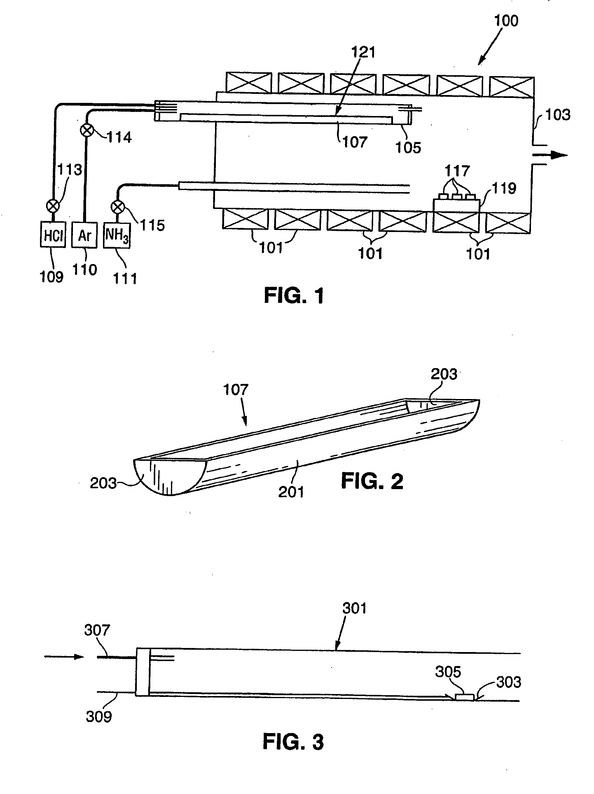
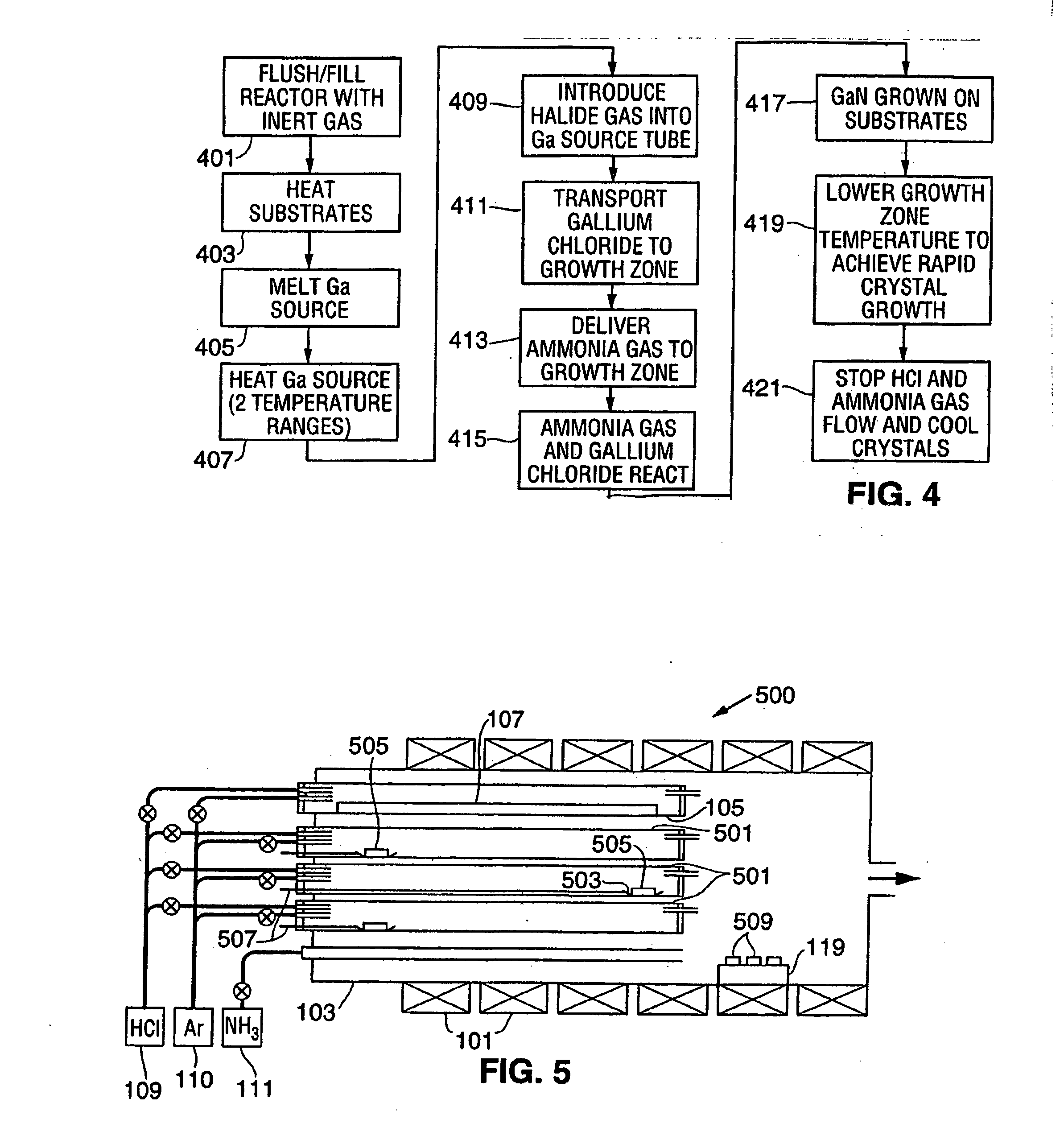
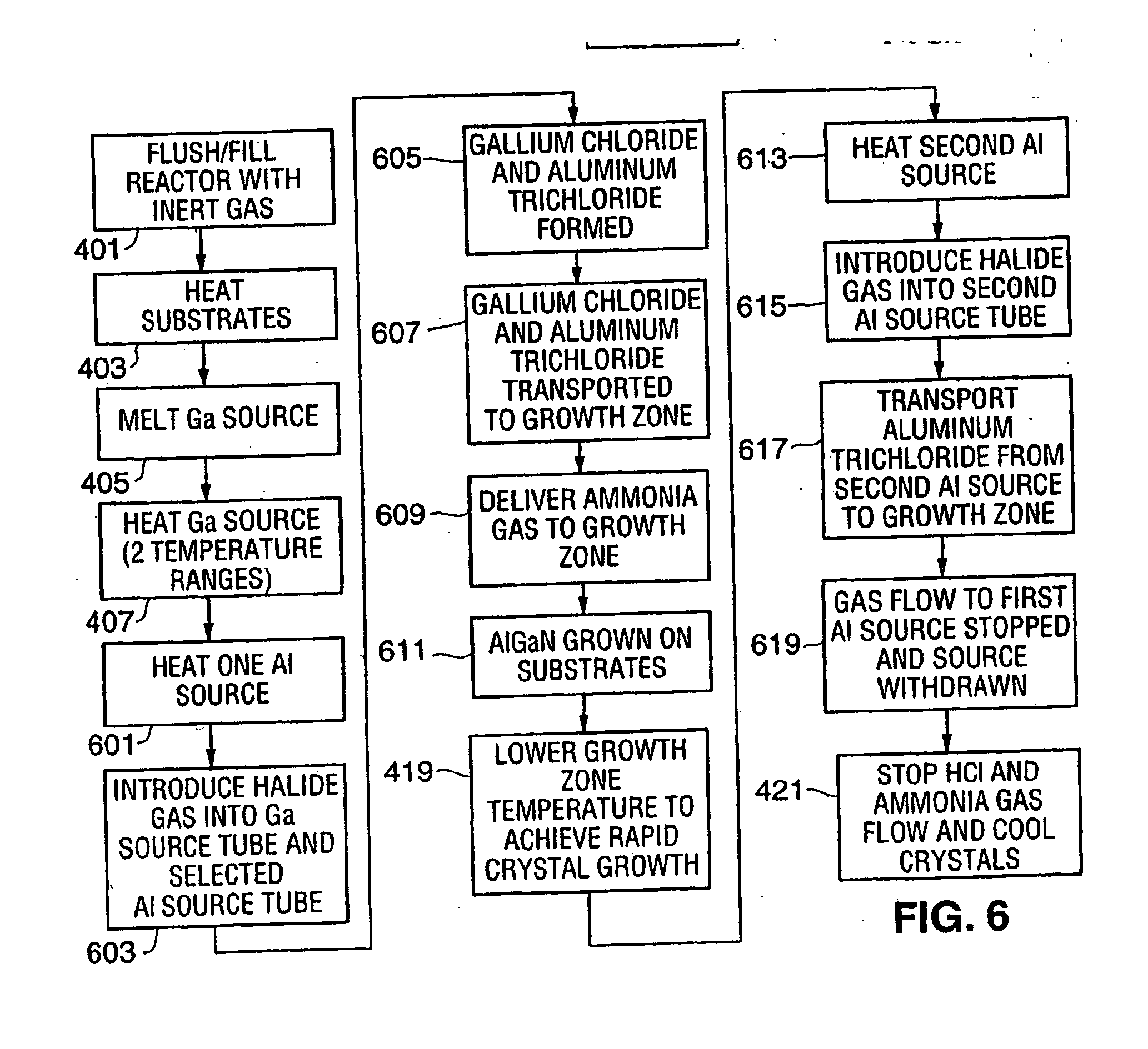
[0069] In this embodiment, multiple SiC substrates of a 6H polytype were loaded into the growth zone of a reactor similar to that shown in FIG. 1. The substrates were placed on a quartz sample holder with the (0001) Si on-axis surface positioned for GaN deposition. One kilogram of Ga metal was positioned in the source boat within the Ga source tube. After purging the reactor with Ar gas to remove air, the growth zone and the Ga source zone were heated to 1100° C. and 650° C., respectively. The majority of the Ga source, however, was maintained at a temperature of less than 100° C., typically in the range of 30°...

embodiment 2

[0080] Embodiment 2

[0081] In this embodiment, a GaN seed was first fabricated as described in Embodiment 1. The 5.08 centimeter diameter (i.e., 2 inch diameter) prepared GaN seed substrates were then placed within a stainless steel, resistively heated furnace and a GaN single crystal boule was grown using a sublimation technique. GaN powder, located within a graphite boat, was used as the Ga vapor source while NH3 gas was used as the nitrogen source. The GaN seed was kept at a temperature of 1100° C. during the growth. The GaN source was located below the seed at a temperature higher than the seed temperature. The growth was performed at a reduced pressure.

[0082] The growth rate using the above-described sublimation technique was approximately 0.5 millimeters per hour. After a growth cycle of 24 hours, a 12 millimeter thick boule was grown with a maximum boule diameter of 54 millimeters. The boule was divided into 30 wafers using a diamond wire saw and the slicing and processing pr...

embodiment 3

[0083] Embodiment 3

[0084] In this embodiment, bulk GaN material was grown in an inert gas flow at atmospheric pressure utilizing the hot-wall, horizontal reactor described in Embodiment 1. Six 5.08 centimeter diameter (i.e., 2 inch diameter) silicon carbide substrates of a 6H polytype, were placed on a quartz pedestal and loaded into a growth zone of the quartz reactor. The substrates were located such that the (0001) Si on-axis surfaces were positioned for GaN deposition. Approximately 0.9 kilograms of Ga (7N) was located within a quartz boat in the Ga source zone of the reactor. This channel was used for delivery of gallium chloride to the growth zone of the reactor. A second quartz tube was used for ammonia (NH3) delivery to the growth zone. A third separate quartz tube was used for HCl gas delivery to the growth zone.

[0085] The reactor was filled with Ar gas, the Ar gas flow through the reactor being in the range of 1 to 25 liters per minute. The substrates were then heated in ...


PUM


Abstract

HVPE method for simultaneously fabricating multiple Group III nitride semiconductor structures during a single reactor run. A HVPE reactor includes a reactor tube, a growth zone, a heating element and a plurality of gas blocks. A substrate holder is capable of holding multiple substrates and can be a single or multi-level substrate holder. The gas delivery blocks are independently controllable. Gas flows from the delivery blocks are mixed to provide a substantially uniform gas environment within the growth zone. The substrate holder can be controlled, e.g., rotated and/or tilted, for uniform material growth. Multiple Group III nitride semiconductor structures can be grown on each substrate during a single fabrication run of the HVPE reactor. Growth on different substrates is substantially uniform and can be performed on larger area substrates, such as 3-12″ substrates.

Description

CROSS-REFERENCE TO RELATED APPLICATIONS [0001] The present application is a continuation-in-part (CIP) of co-pending U.S. application Ser. No. 10 / 632,736, filed on Aug. 1, 2003, which is a continuation of U.S. application Ser. No. 09 / 903,299, filed on Jul. 11, 2001, now U.S. Pat. No. 6,656,285, which is a continuation of U.S. application Ser. No. 09 / 900,833, filed on Jul. 6, 2001, now U.S. Pat. No. 6,613,143, the contents of which are incorporated herein by reference, priority being claimed under 35 U.S.C. §120. The present application also claims priority under 35 U.S.C. §119 to Provisional Application No. 60 / 586,707, filed Jul. 9, 2004, the contents of which are incorporated herein by reference.FIELD OF THE INVENTION [0002] The present invention relates generally to apparatus for processing semiconductor materials and, more particularly, to a HVPE reactor for simultaneously growing multiple uniform Group III nitride semiconductor structures during a single epitaxial growth run. BA...

Claims


Application Information

Patent Timeline
IPC IPC(8): H01L21/20
CPCC30B25/00C30B25/02C30B29/406C30B29/403C30B25/14H01L21/02378H01L21/0254H01L21/02576H01L21/02579H01L21/0262
Inventor DMITRIEV, VLADIMIR A.MASLENNIKOV, VIACHESLAV A.SOUKHOVEEV, VITALIKOVALENKOV, OLEG V.
Owner FREIBERGER COMPOUND MATERIALS
Why Eureka
Try Eureka