Synthesis of germanium sulphide and related compounds

Inactive Publication Date: 2007-04-05
UNIV OF SOUTHAMPTON
View PDF5 Cites 44 Cited by
  • Summary
  • Abstract
  • Description
  • Claims
  • Application Information

AI Technical Summary

Benefits of technology

[0029] Germanium sulphide glass provides not only a important and viable optoelectronic material on its own but through modification of this basic composition through the addition of additional elements, its range of application can be expanded. For example, it is well known that the addition of phosphorous, gallium or arsenic enhances the ability of the glass to be drawn into optical fibre [2]. These glass modifiers are a

Problems solved by technology

These techniques can be useful but in general suffer from problems associated with impurities or difficulty in achieving the desired stoichiometry.
Sealed ampoule melting has a number of disadvantages, in particular the difficulty in obtaining high purity starting materials limits the purity of the resulting glass.
In particular oxygen impurities, carbon and hydrogen resulting from the use of organic compounds, and transition metal ions, all introduce undesirable absorption bands in the transmission spectrum of the glass [2].
Other disadvantages include the difficulty in scaling up the process to large and more economical melt sizes.
Moreover, sealed ampoules when heated can build up dangerously high pressures.
The reaction of, for example, germanium chloride (GeCl4) and hydrogen sulphide (H2S) was deemed unsatisfactory because of a low reaction rate and a low yield of deposited product.
Ge(SC2H5)4] which is unsatisfactory for the production of high purity chalcogenide materials.
Organic materials, containing carbon and hydrogen, result in undesirable CH, SH and other related impurities in the resulting materials [2].
Glass films however were not achieved with this process and the crystalline prod

Method used


Image

  • Synthesis of germanium sulphide and related compounds
  • Synthesis of germanium sulphide and related compounds
  • Synthesis of germanium sulphide and related compounds

Examples


example 1

Thin Film Deposition

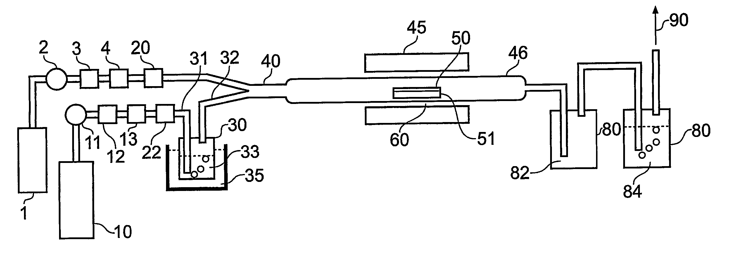
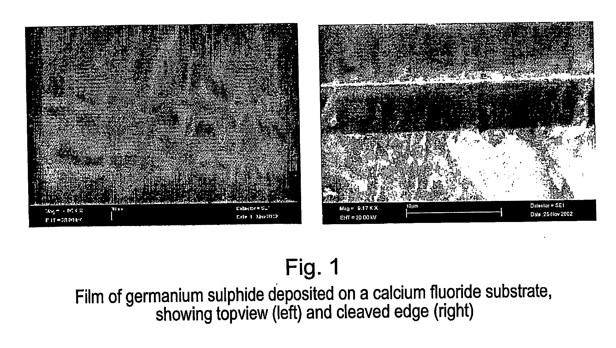
[0099] To illustrate the capability of the process of the present invention for deposition of chalcogenide thin films, germanium sulphide glass thin films were directly deposited onto a planar calcium fluoride substrate using a chemical vapour deposition process as shown in FIG. 1. This invention shows that the reaction of germanium tetrachloride (GeCl4) as a precursor, with hydrogen sulphide (H2S) which is co-delivered with the GeCl4 into a heated furnace, is thermodynamically favourable to produce germanium sulphide glass film at atmospheric pressure and temperatures of about 500° C. Moreover we have demonstrated that the reaction produces germanium sulphide in a glass phase in a single deposition step.

[0100] The reactor used in the experiment is a 16 mm O.D.×500 mm long quartz tube, which is located within a horizontal tube furnace, which is resistively heated. One skilled in the art would recognise this as typical of a hot wall CVD process in which depositi...

example 2

Channel Optical Waveguides

[0107] To illustrate the capability of this invention for the formation of optoelectronic device applications and in particular optical waveguide circuitry capable of guiding and manipulating light channel optical waveguides have been achieved. We have successfully fabricated patterned structures, in this case ridge waveguides in the glass films produced by the process disclosed in this invention.

[0108] Thin films as fabricated in example one were patterned and milled to produce waveguide channels. The process exploited both photolithography and argon ion-beam milling, which one skilled in the art would recognise as an important fabrication prerequisite for optoelectronic circuitry. In the photolithography process, we use a positive Shipley S1813 photoresist and Puddle MF319 developer. One drop of Shipley S1813 photoresist was spin coated at 6000 rpm for 60 seconds on a germanium sulphide thin film. This film was baked at 90° C. for 30 minutes before expo...

example 3

Bulk Glass Fabrication

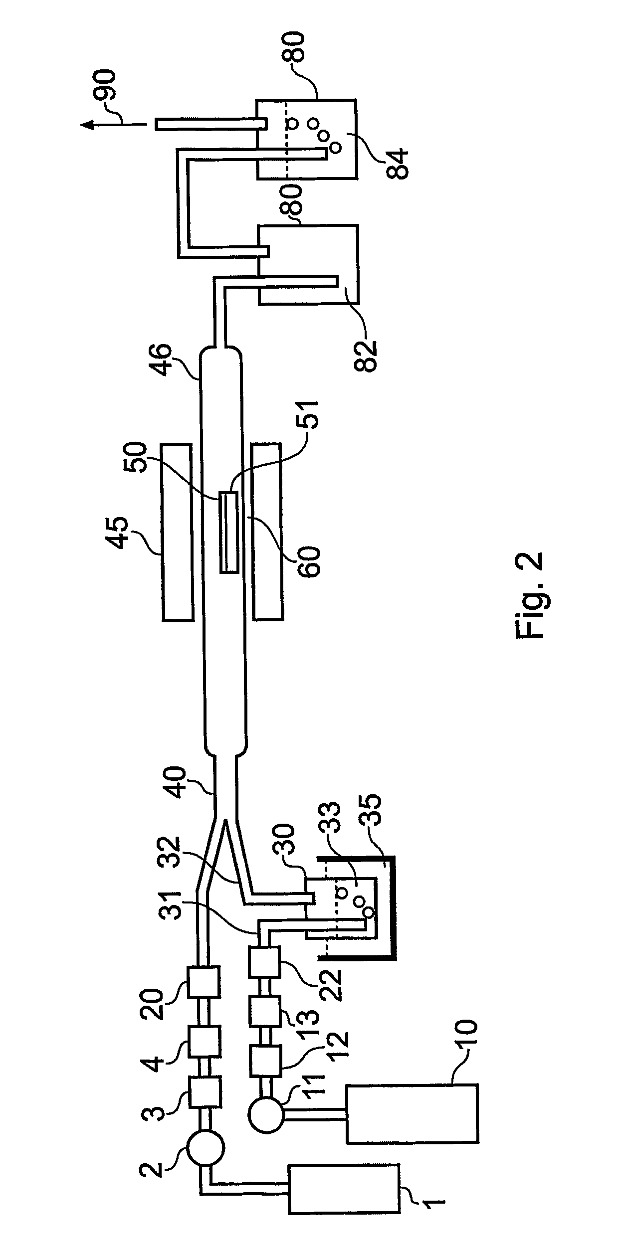
[0112] In this example we show formation of germanium sulphide powder that is melted in situ to form an amorphous solid or bulk glass. The apparatus is illustrated FIG. 8.

[0113] The reactor used in the experiment is a custom build borosilicate chamber of dimensions 50 mm O.D. and 150 mm long that is partially located within a vertical tube furnace that is resistively heated. This is not typical of a conventional CVD reactor that is useful for thin film deposition. Here there is a second collection vessel, which is an integral part of the entire apparatus and which is heated separately and the provision for both an open flowing atmosphere, operating at ambient pressure or slightly above ambient pressure and well as the provision for heating, after the CVD process is completed, to a temperature above the melting temperature of the CVD products.

[0114] During the deposition phase of the experiment, a flow rate for the argon (Ar) carrier gas was 100 ml / min and wa...


PUM

PropertyMeasurementUnit
Temperatureaaaaaaaaaa

Abstract

The invention relates to synthesis of germanium sulphide glasses and optical devices formed therefrom. In a chemical vapour deposition process, germanium tetrachloride is reacted with hydrogen sulphide at temperatures in the range 450-700° C. to form germanium sulphide. Lower temperatures within this range of 450-550° C. directly produce a glass, whereas higher temperatures within the range of 600-700° C. produce a crystalline powder which can then be reduced to a glass by subsequent melting and annealing. The reaction is preferably carried out at atmospheric pressure or slightly higher. Thin films and bulk glasses suitable for optical waveguides can be formed directly in one processing step as can powders and microspheres. The materials synthesised are of a high purity with low oxide impurities and only trace levels of transition metal ions.

Description

BACKGROUND OF THE INVENTION [0001] The invention relates to processes for the synthesis of chalcogenide glass based on germanium sulphide, in particular optical glass for optoelectronic applications. More especially the invention relates to improved methods for the synthesis of the glass and related compounds, apparatus for the same, and to thin films, bulk glass, microspheres and to waveguides, optical fibre preforms, optical fibre and optical devices using such materials. [0002] The production of high purity chalcogenide glasses is essential for a wide range of applications that exploit the material in bulk, thin film, thick film, microsphere and optical fibre form. Applications include infrared transmitting glass and optical fibre, optical data storage using phase change or holographic data storage, infrared windows and lenses for used in, for example, thermal imaging and infrared laser systems, medical applications including endoscopy, telecommunications devices exploiting the l...

Claims


Application Information

Patent Timeline
IPC IPC(8): C03B37/023C03B37/018C03B19/10C03C3/32C03C12/00C03C13/04C03C17/02C23C16/30G02B6/132
CPCC03B19/106C03B37/01807C03B2201/88C03C3/253C03C3/321C03C3/323C03C12/00C03C13/043C03C17/02C23C16/305G02B6/132
Inventor BADDING, JOHN V.HEWAK, DANIEL WILLIAMHUANG, CHUNG-CHE
Owner UNIV OF SOUTHAMPTON
Why Eureka
Try Eureka