Optical element, exposure apparatus using the same, and device manufacturing method

Inactive Publication Date: 2008-05-29
NIKON CORP
View PDF8 Cites 26 Cited by
  • Summary
  • Abstract
  • Description
  • Claims
  • Application Information

AI Technical Summary

Problems solved by technology

With this technology, the exposure of a pattern size of approximately 5 to 70 nm is expected to be available, however, because the refractive index of a substance in this region is close to one, a transmissive refraction type optical element cannot be used unlike in the past and thus a reflection type optical element is used.
Therefore, when the Mo/Si multilayer film is formed on an accurately polished substrate of optical elements, there is a problem that the compressive stress deforms the substrate, causes wavefront aberration in the optical system, and thus deteriorates the optical properties.
However,

Method used


Image

  • Optical element, exposure apparatus using the same, and device manufacturing method
  • Optical element, exposure apparatus using the same, and device manufacturing method
  • Optical element, exposure apparatus using the same, and device manufacturing method

Examples


first embodiment

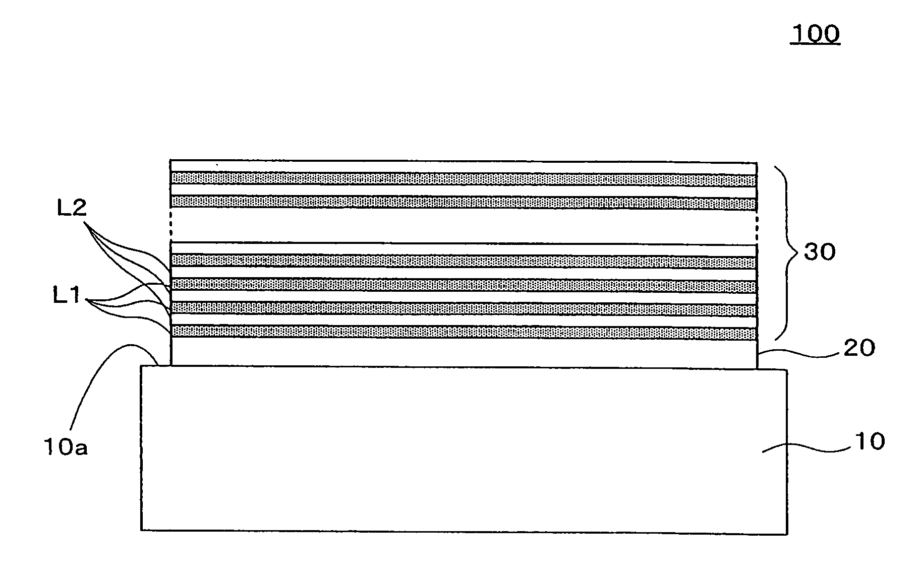
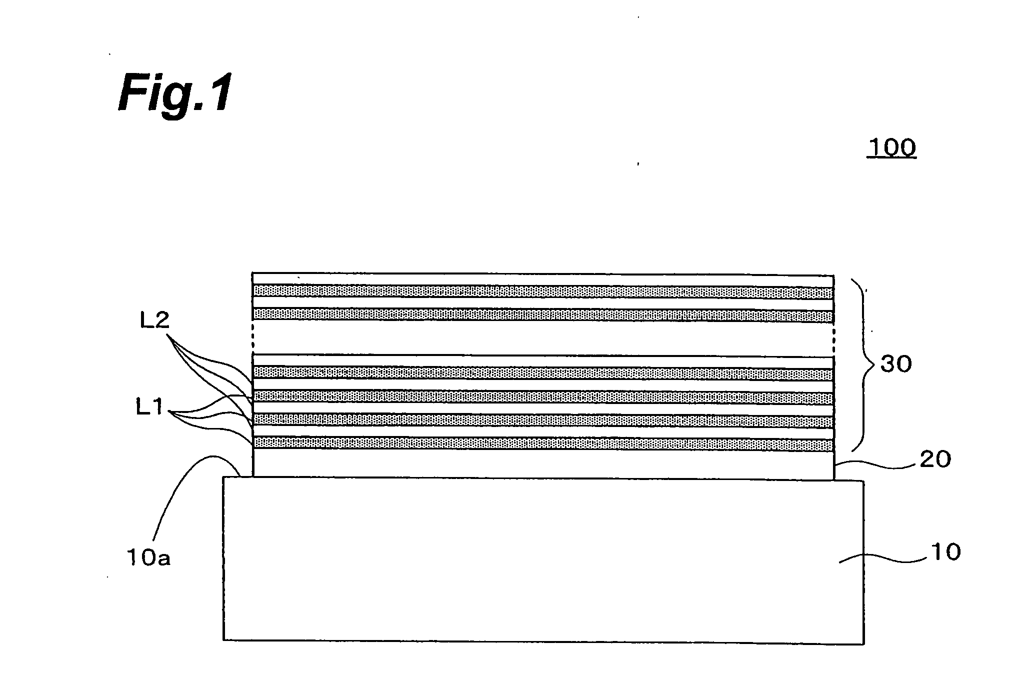
[0024]FIG. 1 is a cross sectional view showing the structure of an optical element concerning a first embodiment. An optical element 100 of this embodiment is a plane reflector, for example, which includes a substrate 10 for supporting a multilayer film structure, a multilayer film 30 for reflection, and an alloy layer 20 for stress relief.

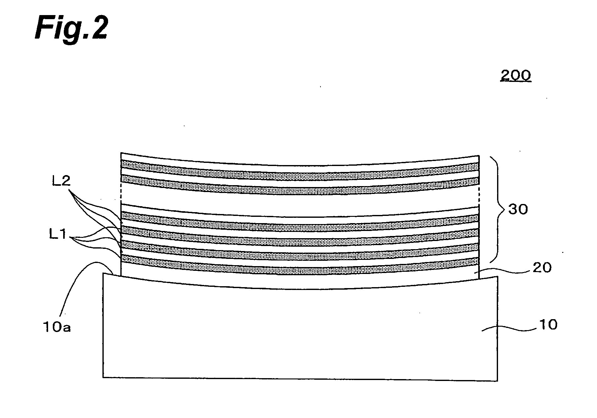
[0025]A lower substrate 10 is formed by processing a synthetic quartz glass or a low expansion glass, for example, and an upper surface 10a thereof is polished into a mirror plane with a predetermined accuracy. The upper surface 10a may be a flat surface as illustrated, but may be a concave surface such as an optical element 200 shown in FIG. 2. Moreover, although illustration is omitted, the upper surface 10a may be a convex surface, a multifaceted surface, or other shaped surface depending on the application of the optical element 100.

[0026]The upper multilayer film 30 is a several to several hundreds layers of thin film formed by alternately de...

second embodiment

[0045]FIG. 3 is a cross sectional view of the structure of an optical element concerning a second embodiment. An optical element 300 of this embodiment is a modification of the optical elements 100 and 200 of the first embodiment shown in FIGS. 1 and 2, and here the same portion is given the same reference numeral to omit the duplicated description. Moreover, the portion not described in particular is the same as the one in the first embodiment.

[0046]In this optical element 300, a resin layer 40 is provided between the alloy layer 20 and the multilayer film 30. This makes the surface of the alloy layer, which is an underlayer of the multilayer film 30, smoother so as not to affect the surface roughness when depositing the multilayer film 30. In addition, the thickness of the resin layer is determined suitably depending on desired reflection characteristics with respect to the optical element 300.

[0047]A polyimide resin can be used as the material constituting the resin layer 40. Spe...

third embodiment

[0049]FIG. 4 is a view for illustrating the structure of an exposure apparatus 400 concerning a third embodiment, which incorporates the optical elements 100, 200, and 300 of the first and second embodiments as the optical component.

[0050]As shown in FIG. 4, this exposure apparatus 400 includes; as the optical system, a light source device 50 for generating extreme ultraviolet light (with a wavelength of 11 to 14 nm); an illumination optical system 60 that illuminates a mask MA with illumination light of extreme ultraviolet light; and a projection optical system 70 that transfers a pattern image of the mask MA to a wafer WA that is a sensitive substrate, and further includes; as a machinery mechanism, a mask stage 81 for supporting the mask MA; and a wafer stage 82 for supporting the wafer WA.

[0051]The light source device 50 includes a laser light source 51 generating a laser beam for plasma excitation, and a tube 52 supplying a gas such as xenon, which is a target material, into an...


PUM


Abstract

There is disclosed an optical element, comprising, a supporting substrate, a multilayer film being supported on the substrate and reflecting extreme ultraviolet light, and an alloy layer provided between the multilayer film and the substrate.

Description

CROSS-REFERENCE TO RELATED APPLICATIONS[0001]This application is based upon and claims the benefit of priority from Japanese Patent Application No. 2006-318441, filed Nov. 27, 2006, and a non-provisional application No. 60 / 935,478, filed on Aug. 15, 2007, the entire contents of which are incorporated herein by reference.BACKGROUND[0002]1. Field[0003]One Embodiments of the present invention relates to an optical element used for extreme ultraviolet light etc., an exposure apparatus using the same, and a device manufacturing method.[0004]2. Description of the Related Art[0005]In recent years, as the semiconductor integrated circuits have become finer, an exposure technology using extreme ultraviolet light, instead of the conventional ultraviolet light, with a wavelength (11 to 14 nm) shorter than that of the conventional ultraviolet light has been developed in order to improve the resolution of an optical system achieved by the diffraction limit of light. With this technology, the exp...

Claims


Application Information

Patent Timeline
IPC IPC(8): G03B27/54G02B5/08
CPCB82Y10/00B82Y40/00G02B5/0891G03B27/54G03F7/70958G03F7/70316G03F7/70783G03F7/70941G03F1/24
Inventor SHIRAISHI, MASAYUKIMURAKAMI, KATSUHIKO
Owner NIKON CORP
Why Eureka
Try Eureka