
All-in-one organic electroluminescent inks with balanced charge transport properties

an electroluminescent ink and all-in-one technology, applied in the field of organic semiconductor devices, can solve the problems of high production cost and low production yield, limited success of the fpd market of the oled, and complex device configuration, and achieve the effect of improving the morphology of the all-in-one organic film

Inactive Publication Date: 2008-06-12
XIAO STEVEN SHUYONG
View PDF1 Cites 52 Cited by
  • Summary
  • Abstract
  • Description
  • Claims
  • Application Information

AI Technical Summary

Benefits of technology

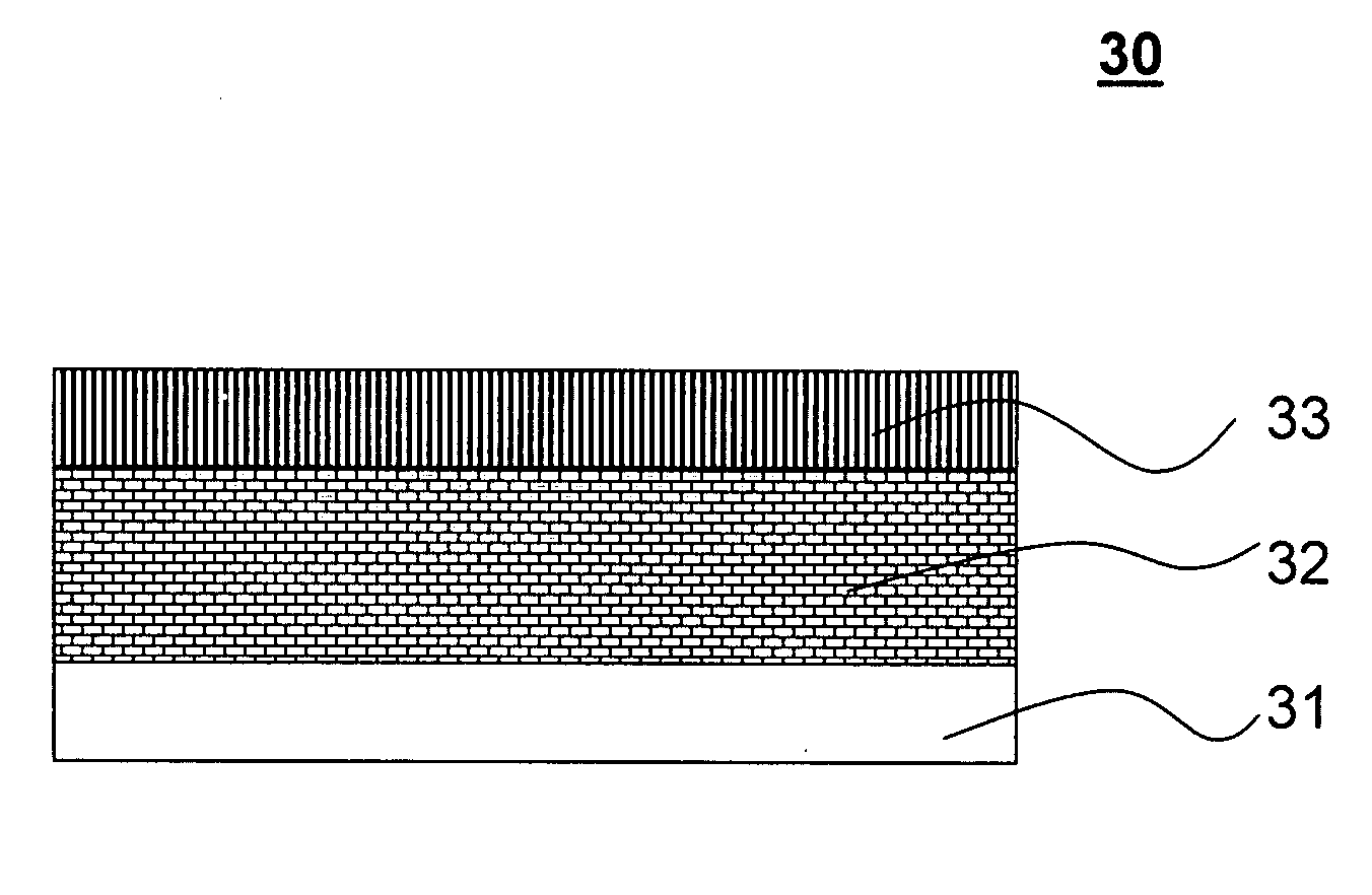
[0012]One objective of the present invention is to provide all-in-one organic electroluminescent inks for the fabrication of single-layer OLED devices. Another objective of the present invention is to provide methods to achieve a balanced charge injection in an all-in-one organic ink by selecting materials and adjusting the relative concentration of the negative charge-transport component and the positive charge-transport component in the all-in-one organic electroluminescent ink. Yet another objective of the present invention is to provide a method to improve the morphology of an all-in-one organic film by adding a binding component into the all-in-one organic electroluminescent ink. Still another objective of the invention is to provide a solution process to fabricate single-layer OLED devices by using the all-in-one organic electroluminescent inks.

Problems solved by technology

Despite these development works, OLED has achieved limited success in flat panel display (FPD) marketplace due to its high production cost and low production yield.
The high production cost and low production yield are direct consequences of two problems associated with the OLED technology.
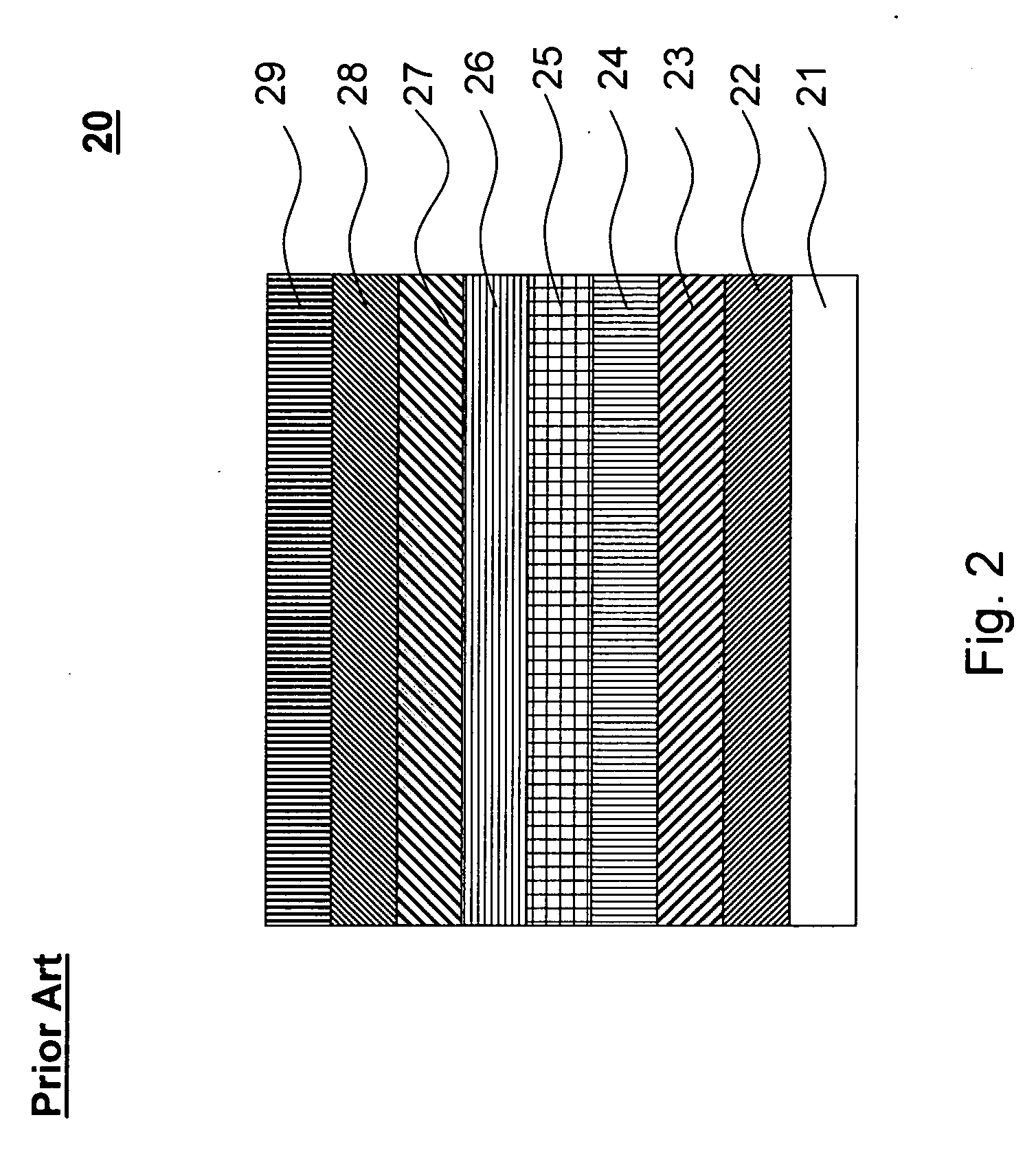
One problem is complexity of the device configuration.
While improving the performance of the multilayer OLED configuration, researchers are introducing more layers of materials into this configuration and making the structure even more complex.
Fabrication of such complicated multiplayer devices is often tedious, difficult and expensive.
The second problem of the multilayer OLED technology is high cost and low yield of the fabrication process.
To set-up and maintain a high vacuum in working condition is very costly.
Furthermore, the vacuum deposition rate is low.
As an overall consequence of these two problems, a huge initial capital investment on machinery is always involved to start any OLED production line.
Furthermore, the production throughput is generally low and the production capability is limited by the size of the vacuum chambers involved.
All these add into the cost of the final product, making this technology less competitive with the existing technologies such liquid crystal display (LCD), and plasma display panel (PDP) in flat panel display (FPD).
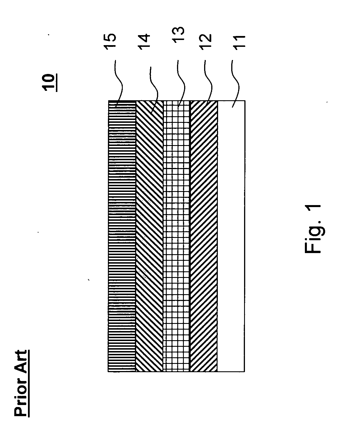
Practically, however, no such a light emitting material can yield an efficient conversion from carriers to photons under this simple structure.
This is because the light emitting materials are often ineffective in extracting charge carriers from the electrodes and in transporting both charge carriers so that the holes and electrons are met and recombined to release photons.
Because it takes an electron hole pair (one electron and one hole) to recombine to generate one photon, light generation is limited by the densities of the two types of populated charge carriers (electron or hole).
The OLED device (10) is generally not very efficient in converting electricity to light.

Method used


Image

  • All-in-one organic electroluminescent inks with balanced charge transport properties
  • All-in-one organic electroluminescent inks with balanced charge transport properties
  • All-in-one organic electroluminescent inks with balanced charge transport properties

Examples


example 1

Synthesis of an Electro-Luminescent Compound, DPVBi

4,4′-Bis[(diethyl phosphate)methyl]biphenyl

[0047]Under nitrogen atmosphere, 25.12 g of 4,4′-bis(chloromethyl)-1,1′-biphenyl (100 mmol.) and 100 ml of triethyl phosphite were charged together in a dried 3-neck flask (250 ml) equipped with a reflux condenser, a gas inlet, and an electronic thermometer. It immediately caused a beige suspension. The suspension was heated and stirred for two hours at 130° C. The solution was continued to be stirred for another four hours at 130° C. After it cooling down to room temperature, it was kept in a refrigerator for overnight. The resulting gray precipitate was filtered, thoroughly washed with cool hexane (5×50 ml), and dried under suction and then put in a vacuum oven for two hours at 65° C. Finally, 39.43 g of a beige crystal was collected (86.8%).

Characterization of the Crystal:

[0048]m.p.: 103-109° C.

[0049]FTIR (KBr, cm−1): 3041, 2980, 14995, 14405, 1392, 1245, 1035, 961, 864, 831, 772, 736, 5...

example 2

Synthesis of Electron-Transport Component, OVI588

1,3,5-tris(4-flluorobiphenyl-4′-yl)benzene

[0058]In 3-neck round-bottom flask (250 ml) filled with nitrogen, 100 ml of freshly-distilled THF and 20 ml of de-ionized water were poured and degassed with nitrogen bubbles for 30 minutes. 0.78 g of tetramethylamonium bromide was added as a phase transfer agent. 0.33 g of palladium acetate and 1.8 g of triphenylphosphine were added and the resulting suspension was stirred for a half of hour to activate the catalysts. 2.42 g of 1,3,5-tris(4-bromophenyl)benzene and 2.65 g of 4-fluorophenylboronic acid were then added and the resulting mixture was heated to reflux before adding 7.2 g of sodium carbonate. The solution was heated to reflux for 48 hours to complete the reaction. After cooled down to room temperature, the reaction mixture was transferred into a separation funnel and water was separated. The separated organic layer was again washed by water (2×20 ml) and dried with sodium sulfate an...

example 3

Synthesis of Hole-Transport Material, OVI544

9-(4-methoxyphenyl)carbazole

[0059]A 1,000 ml 3-neck flask equipped with a Dean Starks trap, a water condenser and a magnetic stirrer was flame dried with a torch under nitrogen and cooled down to room temperature. 300 ml of anhydrous o-xylene was poured into the flask and degassed with nitrogen bubble for 30 minutes. 41.8 g of carbazole and 58.51 g of 4-iodoanisole were added and heated to yield a clear brown solution. 2.48 g of copper chloride and 4.5 g of 1,10-phenanthroline were then added, followed by 14.1 g of potassium hydroxide. After refluxed for 3 hours, another 14.1 g of potassium hydroxide was added and the resulting mixture was continued to reflux for another 20 hours and it was cool down to room temperature. After the reaction mixture was transferred into a separation funnel, it was washed by water (3×100 ml), dried with sodium sulfate and filtered to yield 46.3 g of flakes. 39.5 g of final product was obtained after a re-crys...


PUM

PropertyMeasurementUnit
Volumeaaaaaaaaaa
Volumeaaaaaaaaaa
Volumeaaaaaaaaaa

Abstract

The present invention discloses all-in-one organic electroluminescent inks for balanced charge injection. When of single layer organic lighting emitting diodes are made from these inks, the charge balance can be readily achieved. By using the invented all-in-one organic electroluminescent inks, both the device structure and the fabrication process are simplified, which will increase the production yield and reduce the production cost in manufacturing such devices. This invention also teaches methods to fabricate single layer all-in-one organic light emitting diodes.

Description

FIELD OF THE INVENTION[0001]This invention relates to organic semiconductor devices for optoelectronic applications. More specifically, it relates to all-in-one organic electroluminescent inks with balanced charge injection for single-layer organic light emitting device fabrication.BACKGROUND OF THE INVENTION[0002]Organic light emitting diode (OLED) in flat panel display (FPD) applications offers advantages of bright color, high contrast, wide view angle, high energy efficiency, light weight and small thickness.[0003]The commercialization of current OLED technology is driven by the earlier invention of Tang et al (U.S. Pat. Nos. 4,769,292 and 4,885,211, where a three layer OLED composing of a hole-transporting layer (HTL), an organic light-emitting layer (LEL) and an electron-transporting layer (ETL) was disclosed). Since this invention, more layers of materials with different functionalities are added to this three layer device structure to improve its performance in color, stabili...

Claims


Application Information

Patent Timeline
IPC IPC(8): C09K11/06
CPCC09K11/06C09K2211/1029C09K2211/185H05B33/14H01L51/0081H01L51/0085H01L51/5012H01L51/0042
Inventor QIU, CHUNONGXIAO, STEVEN SHUYONGQIU, CINDY X.
Owner XIAO STEVEN SHUYONG
Learn More