Refractory metal-doped sputtering targets, thin films prepared therewith and electronic device elements containing such films

a technology of refractory metal and sputtering target, which is applied in the direction of diaphragms, metallic material coating processes, conductive materials, etc., can solve the problems of reducing throughput, increasing materials, equipment and manpower, and voids and other deleterious defects, etc., to achieve the effect of reducing diffusion and resistivity

Inactive Publication Date: 2009-07-23
GLAS TRUST +1
View PDF5 Cites 14 Cited by
  • Summary
  • Abstract
  • Description
  • Claims
  • Application Information

AI Technical Summary

Benefits of technology

[0019]In certain preferred embodiments of the invention, the refractory dopant component can be segregated into grain boundaries likely due to the relative insolubility of the refractory metals in the conductive matrix metal, particularly Cu. Grain boundaries are diffusion channels in materials, where defects and vacancies are more prevalent than within the grains. Vacancy diffusion is widely presumed to be the most important mechanism for diffusion. Refractory metal atoms present at grain boundaries can thus help block the diffusion channels and reduce diffusion. Additionally, resistivity remains low since the refractory dopant component is present in a small quantity.

Problems solved by technology

Hillocks, voids and other deleterious defects can form in the Al or Cu thin films and / or at the interfaces and impair the operability of the devices or circuits (e.g., short circuits).
The addition of an extra layer in the architecture of the device increases cost of materials, equipment and manpower and reduces throughput.
Moreover, as the critical dimension employed in semiconductor IC fabrication continues to rapidly decrease to 45 nm, 32 nm and so on, the use of barrier layers will become prohibitive as spatial demands will not be able to be achieved.
Unfortunately, neither material has sufficient reduction in diffusivity and the necessary conductivity.

Method used


Image

  • Refractory metal-doped sputtering targets, thin films prepared therewith and electronic device elements containing such films
  • Refractory metal-doped sputtering targets, thin films prepared therewith and electronic device elements containing such films
  • Refractory metal-doped sputtering targets, thin films prepared therewith and electronic device elements containing such films

Examples


examples 1-4

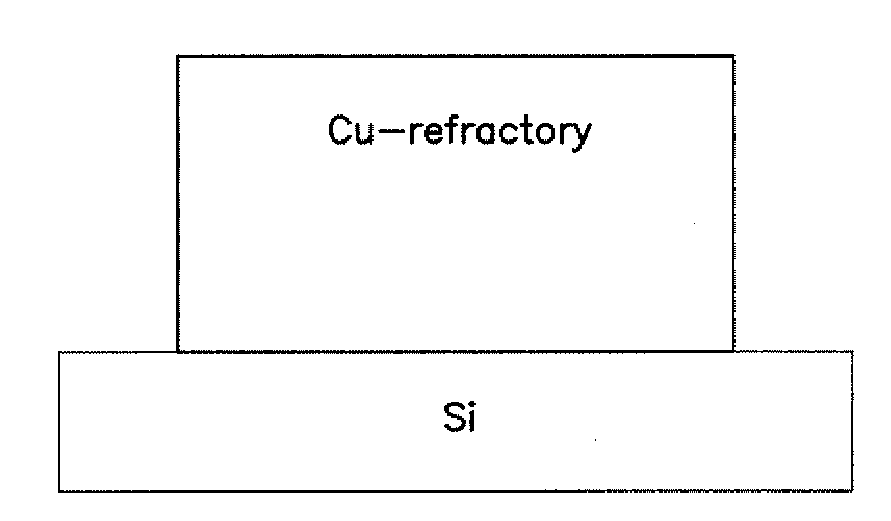
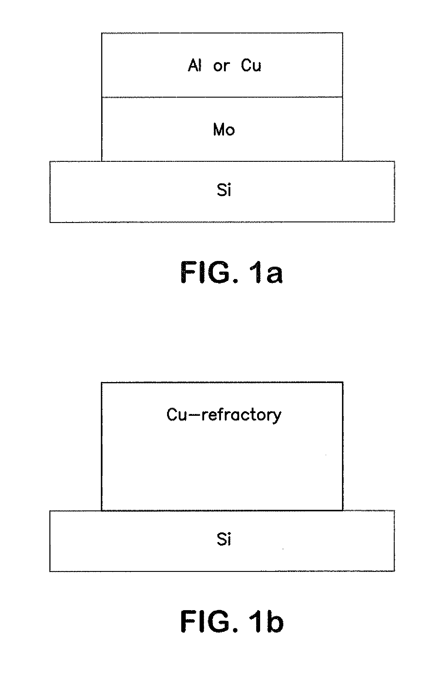
Control, Examples 1-4 and Comparative Examples 5-7

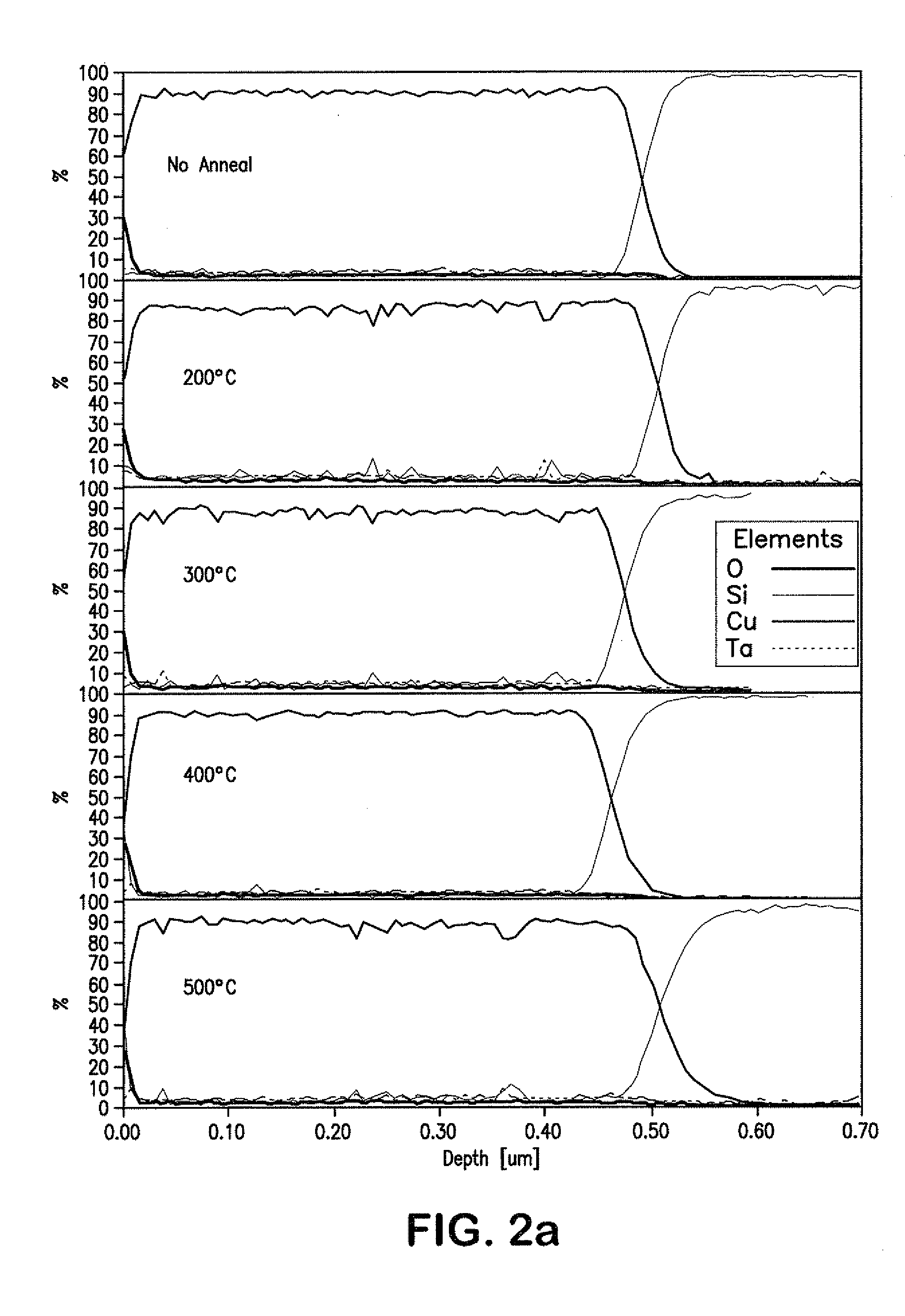
Thin Film Evaluation

[0070]Initially, a copper powder was provided (Control Sample, Pure Cu) and seven powders were prepared (Inventive Example 1, Cu—Ta; Inventive Example 2, Cu—Cr; Inventive Example 3, Cu—Ta / Cr; Inventive Example 4, Cu—Ni; and Comparative Examples 5, 6 & 7, Cu—Mo, Cu—W and Cu—Ta / Si, respectively) by dry blending copper powder, CuLox® type 620, normal 20 μm (commercially available from CuLox Technologies, Inc., Naugatuck, Conn.), with Ta, Cr, Ni, Si, Mo and / or W powder, as designated above, in amounts of 0.1 to 6% by weight. The tantalum powder used was H. C. Starok NH230 capacitor grade powder, available from H. C. Starck, Inc. Newton, Mass.). The chromium powder used was 325-mesh powder commercially available from Alfa / Aesar. The molybdenum powder used was H. C. Starek type MMP-OMFP, normal 5 μm, available from H. C. Starok, Inc. (Newton, Mass.). The tungsten powder used was H. C. Starck WMP normal 3.5 μm, available...


PUM

PropertyMeasurementUnit
temperatureaaaaaaaaaa
pressureaaaaaaaaaa
temperatureaaaaaaaaaa

Abstract

Metallic materials consisting essentially of a conductive metal matrix, preferably copper, and a refractory dopant component selected from the group consisting of tantalum, chromium, rhodium, ruthenium, iridium, osmium, platinum, rhenium, niobium, hafnium and mixtures thereof, preferably in an amount of about 0.1 to 6% by weight based on the metallic material, alloys of such materials, sputtering targets containing the same, methods of making such targets, their use in forming thin films and electronic components containing such thin films.

Description

CROSS-REFERENCE TO RELATED APPLICATIONS[0001]This application claims priority to and benefit of, under 35 U.S.C. §119(e), U.S. Provisional Patent Application No. 60 / 982,163, filed on Oct. 24, 2007, the entire contents of which are hereby incorporated herein by reference.BACKGROUND OF THE INVENTION[0002]Aluminum (Al) thin films are widely used in flat panel displays as conducting wires and electrodes. The substrate is normally glass (SiO2, silicon dioxide). Copper (Cu) thin films are generally used in semiconductor integrated circuits for interconnect wires with silicon (Si) as a substrate. During normal device processing, the temperature can be raised to 250° C., and even as high as 500° C. At such temperatures, Al and Cu can diffuse into Si or SiO2 substrates, and Si can likewise diffuse into the Al or Cu films. Hillocks, voids and other deleterious defects can form in the Al or Cu thin films and / or at the interfaces and impair the operability of the devices or circuits (e.g., shor...

Claims


Application Information

Patent Timeline
Patent Type & Authority Applications(United States)
IPC IPC(8): C23C14/14C23C14/35C23C14/06B22F1/00
CPCC22C1/002C22C1/0425C22F1/08H01B1/026C23C14/3414H01B1/02C23C14/14Y10T428/31678B22F2998/10C22C1/11B22F1/09B22F3/02B22F3/10B22F3/15
Inventor SUN, SHUWEIGAYDOS, MARKWU, RICHARDKUMAR, PRABHAT
Owner GLAS TRUST
Why Eureka
Try Eureka