Electroconductive layer, laminate using the same, and producing processes thereof

Active Publication Date: 2009-08-06
MEC CO LTD
View PDF11 Cites 11 Cited by
  • Summary
  • Abstract
  • Description
  • Claims
  • Application Information

AI Technical Summary

Benefits of technology

[0045]The above has described one of preferred embodiments; however, the invention is not limited to the embodiment. For example, with the reference to FIGS. 1A to 1D, an example using the plate-form copper layer 1 has been described; however, a copper wiring pattern layer may be used as the copper layer.
[0046]Further, in FIG. 1D, the flat resin layer 4 is illustrated; however, as the resin layer, for example, a solder resist pattern layer may be used. Also in this case, the copper-tin alloy layer naked from openings in the solder resist can easily be removed while the bondability between the electroconductive layer and the solder resist is certainly retained. Additionally, diffusion of tin can be prevented since the copper-tin alloy layer in the invention is far thinner than conventional copper-tin alloy layers. Thus, the copper-tin alloy layer naked from the openings is easily removed even after a long time elapses from the end of the formation of the copper-tin alloy layer. As the solution for removing the copper-tin alloy layer, concentrated nitric acid, a nitric-acid/hydrogen-peroxide based etching agent, an iron chloride based etching agent, or any other removing solution in which copper-tin alloy can be dissolved may be used. From the viewpoint of preventing the copper layer from bei

Problems solved by technology

Further, in particular, in the case of using the so-called hard resin, which has a high glass transition temperature, an effect of improving the bondability between the copper layer and the resin layer is insufficient in some cases.
Moreover, in a case where tin needs to be removed in a subsequent step, the removal thereof is difficult since the tin layer usually has a thickness of 1 μm or more.
At this time, tin may hinder the plating treatment; thus, it is necessary to remove tin by etching or the like.
As a result, there is caused a problem that a wiring pattern in the solder resist opening may be made thin.
As a result, with the passage of time, the removal of the tin layer or the copper-tin alloy layer may become difficult.
Even if the surface of an ordinary tin layer is treated with a silane compound as in JP-A-1-109796, the bondability thereof t

Method used


Image

  • Electroconductive layer, laminate using the same, and producing processes thereof
  • Electroconductive layer, laminate using the same, and producing processes thereof
  • Electroconductive layer, laminate using the same, and producing processes thereof

Examples


Example

Example 1

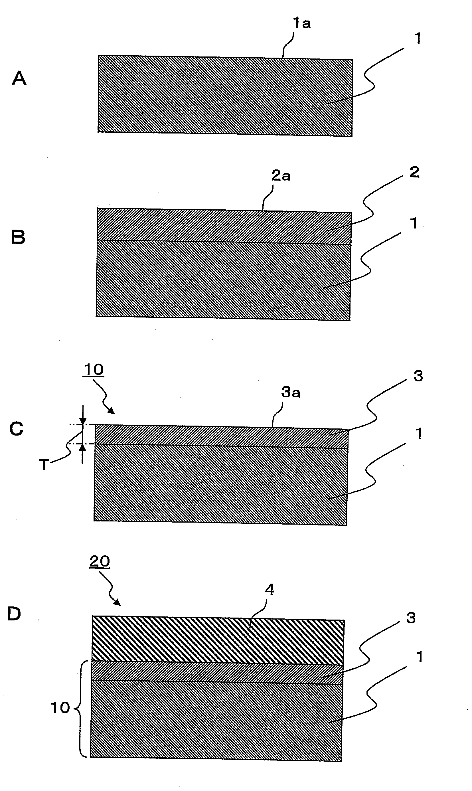
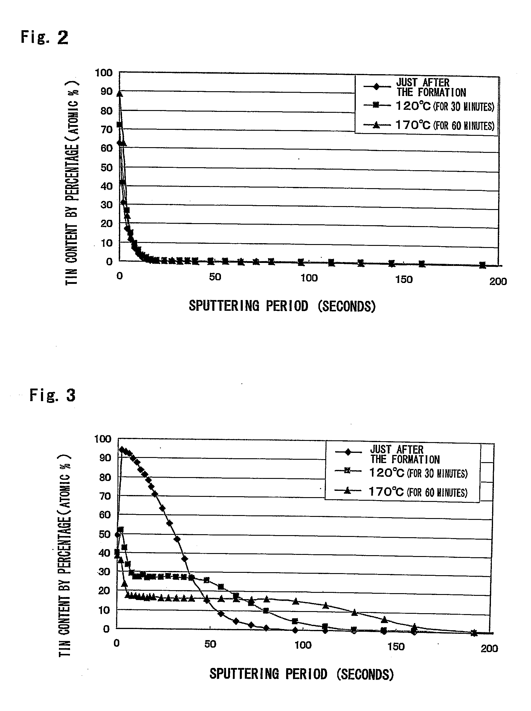
[0049]A substrate wherein a copper electroplating layer 17 μm in thickness was formed on a copper-clad laminated plate (glass epoxy multi R-1766, manufactured by Matsushita Electric Industrial Co., Ltd.; copper foil piece thickness: 35 μm) was cut into a size of 100 mm×100 mm. This was immersed in a 10% by mass sulfuric acid solution for 30 seconds to clean the surface of the copper plating layer. The substrate was rinsed with water and then dried. The resultant was used as a test substrate. This test substrate was subjected to swinging immersion treatment in a displacement tin plating solution (T-9900) manufactured by Mec Co., Ltd. at 30° C. for 30 seconds. Thereafter, the substrate was rinsed with water, and then a tin plating treated layer was formed on the surface of the copper electroplating layer. Immediately after the formation, the tin plating treated layer was subjected to swinging immersion treatment in a 0.67% by mass solution of nitric acid in water at 30° C. f...

Example

Example 2

[0054]A tin plating treated layer was formed on the same test substrate as in Example 1 in the same manner as in Example 1, and the substrate was immediately immersed into hot water at 30° C., and allowed to stand still therein for one minute. Thereafter, the tin plating treated layer was immediately subjected to swinging immersion treatment in a 0.67% by mass solution of nitric acid in water at 30° C. for 20 seconds to remove a surface region of the tin plating treated layer. The resultant was then rinsed with water, and dried to form a copper-tin alloy layer. Then, in the same manner as in Example 1, the resultant was evaluated about the individual items.

Example

Examples 3 to 11

[0055]The temperature of the hot water and the period for the immersion in Example 2 were changed to each temperature and each period in Table 1. In the same manner as in Example 2 except the change, samples of Examples 3 to 11 were yielded. The samples were evaluated in the same manner as in Example 1 about the individual items.


PUM

PropertyMeasurementUnit
Temperatureaaaaaaaaaa
Timeaaaaaaaaaa
Percent by massaaaaaaaaaa

Abstract

The object of the present invention is to provide an electroconductive layer that retains bondability to a resin layer certainly and is further a layer from which a copper-tin alloy layer is easily removed in a subsequent step, a laminate using this layer, and producing processes thereof. The electroconductive layer of the present invention is an electroconductive layer which is to be bonded to a resin layer, and which contains a copper layer and a copper-tin alloy layer laminated over the copper layer, wherein the copper-tin alloy layer has a thickness of 0.001 to 0.020 μm.

Description

BACKGROUND OF THE INVENTION[0001]1. Field of the Invention[0002]The present invention relates to an electroconductive layer which is to be bonded to a resin layer, a laminate using this layer, and producing processes thereof.[0003]2. Description of Related Art[0004]Ordinary multilayer wiring boards are each produced by laminating / pressing an inner layer substrate having, on its surface, an electroconductive layer made of copper onto a different inner layer substrate and / or a copper foil with a prepreg interposed therebetween. Their electroconductive layers are connected electrically to each other through a penetrating hole having a hole-wall plated with copper, which is called a through hole. On the electroconductive layer surface of the inner layer substrate, for example, a copper oxide in a needle form, which is called black oxide or brown oxide, may be formed in order to improve the bondability to the prepreg. According to this manner, the needle-form copper oxide penetrates the ...

Claims


Application Information

Patent Timeline
IPC IPC(8): B32B15/08C25D5/56
CPCH05K3/384H05K3/388H05K2201/0355H05K2203/0353Y10T428/12569Y10T428/12431Y10T428/12493Y10T428/12708H05K2203/0361H01L21/203H05K3/38
Inventor KAWAGUCHI, MUTSUYUKISAITO, SATOSHIAMATANI, TSUYOSHIFUJII, YUKO
Owner MEC CO LTD
Why Eureka
Try Eureka