

Dielectric film and semiconductor device using dielectric film
- Summary
- Abstract
- Description
- Claims
- Application Information
AI Technical Summary
Benefits of technology
Problems solved by technology
Method used
Image

Examples
first example
Example using Cosputtering
[0104]A first example of the present invention will now be described in detail with reference to the drawings.
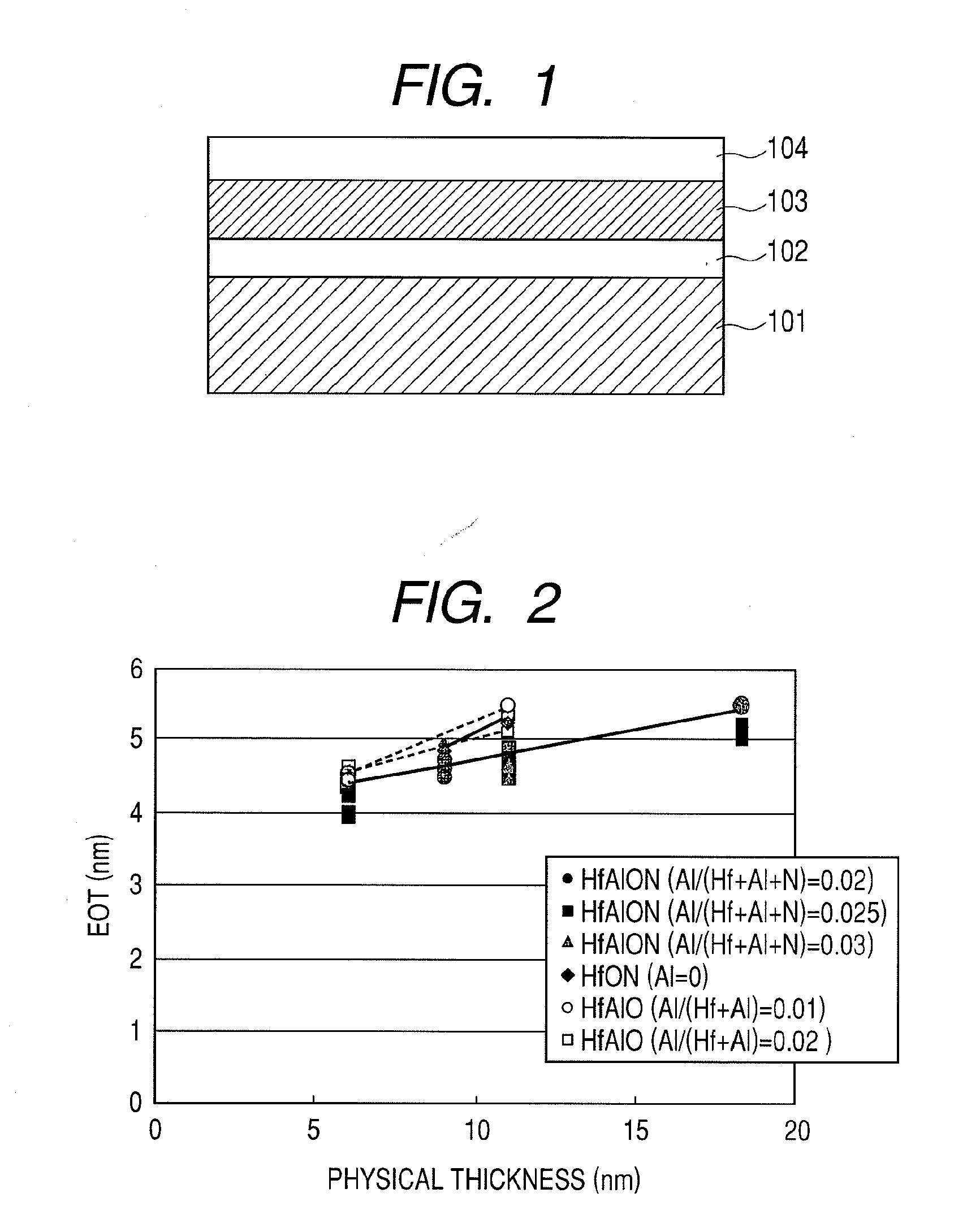
[0105]FIG. 1 is a diagram illustrating an MIS capacitor having the dielectric film 103. A HfAlON film was deposited by a sputtering method as the dielectric film 103 on the silicon substrate 101 having the silicon dioxide film 102 with a film thickness of 3 to 5 nm on a surface thereof. Metallic targets of Hf and Al were used as targets. Argon, oxygen, and nitrogen were used as sputter gases. In other words, a substrate processing apparatus according to the present example includes, in a first chamber thereof, a supplying mechanism that supplies a Hf target, an Al target, and a sputter gas into the first chamber. More specifically, the substrate processing apparatus according to the present example includes a first physical vapor deposition mechanism for performing physical vapor deposition such as sputtering using a Hf target and an Al target.
[0106...
second example
Example using ALD Method and CVD Method
[0125]The present example differs from the first example in that the dielectric film 103 is formed by a CVD method or an ALD method. Other formation processes are the same as the first example. Therefore, a substrate processing apparatus according to the present example includes a mechanism for realizing at least one of a CVD method and an ALD method such as a supplying mechanism that supplies an organic metallic material and an oxidant into a chamber.
[0126]A HfAlON film was formed as the dielectric film 103 by a CVD method or an ALD method at a range of 5 nm to 25 nm on the substrate 101 having the silicon dioxide film 102 on a surface thereof. A substrate temperature was set to 300° C., trimethylaluminum (Al(CH3)3) and tetrakis(diethylamino)hafnium (Hf[(C2H5)2N]4) were used as organic metallic materials, and H2O was used as an oxidant. The method of forming a dielectric film can be set by controlling a partial pressure of the oxidant to be in...
third example
Example Applied to Gate Insulating Film
[0138]A third example of the present invention will now be described in detail with reference to the drawings.
[0139]FIG. 16 is a diagram illustrating processes of a semiconductor device manufacturing method according to a third example of the present invention.
[0140]First, as depicted by process 1 in FIG. 16, a substrate processing apparatus according to the present example forms an element isolation region 302 on a surface of a silicon substrate 301 using a STI (shallow trench isolation) technique. The substrate processing apparatus according to the present example then forms a silicon dioxide film 303 with a film thickness of 1.8 nm on the element-isolated surface of the silicon substrate using a thermal oxidation method. Subsequently, the substrate processing apparatus according to the present example forms a HfAlON film with a film thickness ranging from 1 nm to 10 nm as a dielectric film 304 using the same method as the first example or th...
PUM
| Property | Measurement | Unit |
|---|---|---|
| Temperature | aaaaa | aaaaa |
| Temperature | aaaaa | aaaaa |
| Fraction | aaaaa | aaaaa |
Abstract
Description
Claims
Application Information