Method for manufacturing semiconductor device

a manufacturing method and semiconductor technology, applied in the direction of manufacturing tools, solid-state devices, transistors, etc., can solve the problems of metal diffused into the semiconductor film, adversely affecting the adverse effects of the semiconductor element such as the increase of the off-current of the thin-film transistor, so as to suppress the deterioration of the characteristics of the semiconductor element, suppress the reduction of yield, and suppress the effect of yield

Inactive Publication Date: 2011-03-03
SEMICON ENERGY LAB CO LTD
View PDF17 Cites 15 Cited by
  • Summary
  • Abstract
  • Description
  • Claims
  • Application Information

AI Technical Summary

Benefits of technology

[0018]In addition, deposition rate at the time of forming the insulating film containing nitrogen by plasma nitridation generally tends to be low in comparison with the case where an evaporation method such as a CVD method is employed. However, when the insulating film containing nitrogen formed by plasma nitridation has a thickness of at least 3 nm or more, the insulating film containing nitrogen has an effect of preventing impurities such as metal from diffusing into the semiconductor film. Such a thickness does not need a long treatment time for plasma nitridation. Specifically, the thickness of the insulating film containing nitrogen is 3 nm to 20 nm, preferably, 3 nm to 5 nm.
[0019]After the above SOI substrate is formed, the thin semiconductor fi

Problems solved by technology

In particular, when laser light irradiation is performed in order to improve the crystallinity of the semiconductor film which is damaged in a separation step, the above metal contained in the glass substrate significantly diffuses into the semiconductor film.
It is known that if there is a metal such as Cu or Fe on the surface of the semiconductor film, characteristics of a semiconductor elem

Method used


Image

  • Method for manufacturing semiconductor device
  • Method for manufacturing semiconductor device
  • Method for manufacturing semiconductor device

Examples


embodiment 1

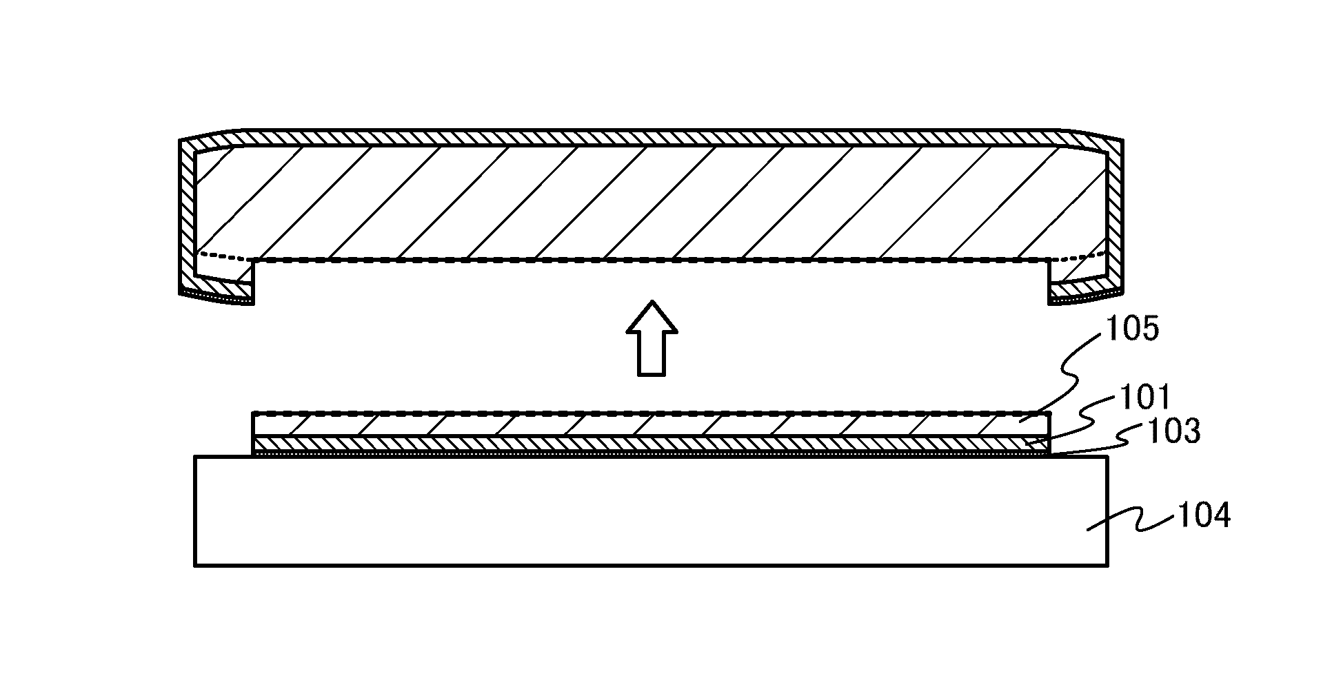
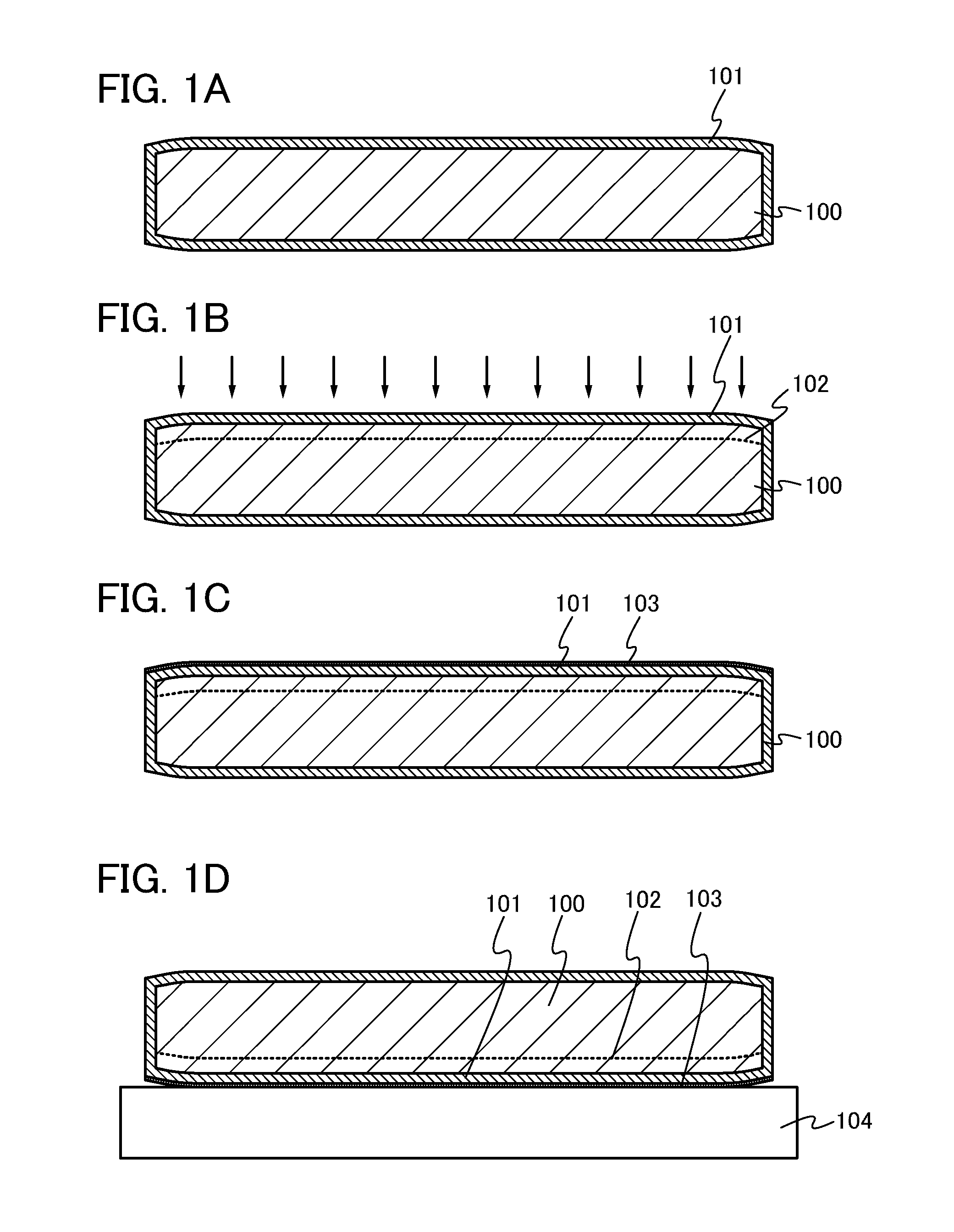
[0037]In this embodiment, methods for manufacturing an SOI substrate and a semiconductor device according to an embodiment of the present invention will be described.

[0038]As illustrated in FIG. 1A, a bond substrate 100 is cleaned and then an oxide film 101 is formed over the bond substrate 100.

[0039]As the bond substrate 100, a single crystal semiconductor substrate formed using silicon, germanium, or the like can be used. Alternatively, a single crystal semiconductor substrate formed using a compound semiconductor such as gallium arsenide or indium phosphide can be used as the bond substrate 100. Further alternatively, a semiconductor substrate formed using silicon having crystal lattice distortion, silicon germanium in which germanium is added to silicon, or the like may be used as the bond substrate 100.

[0040]Note that in a single crystal semiconductor substrate used for the bond substrate 100, the directions of crystal axes are preferably uniform; however, the substrate is not ...

embodiment 2

[0112]In this embodiment, methods for manufacturing an SOI substrate and a semiconductor device in which the insulating film 103 is formed before the formation of the embrittlement layer 102 will be described.

[0113]First, similarly to Embodiment 1, the bond substrate 100 is cleaned, and then the oxide film 101 is formed over the bond substrate 100, as shown in FIG. 3A.

[0114]Next, as shown in FIG. 3B, plasma is generated under an atmosphere of a gas containing nitrogen atoms and plasma nitridation is performed on the surface of the oxide film 101, so that the insulating film 103 containing nitrogen atoms is formed over the oxide film 101. The composition of the insulating film 103 is determined depending on materials which form the bond substrate 100 and the oxide film 101. Specifically, the insulating film 103 includes a semiconductor such as silicon or germanium in addition to nitrogen atoms as its composition; for example, the insulating film 103 is a silicon nitride film, a silic...

embodiment 3

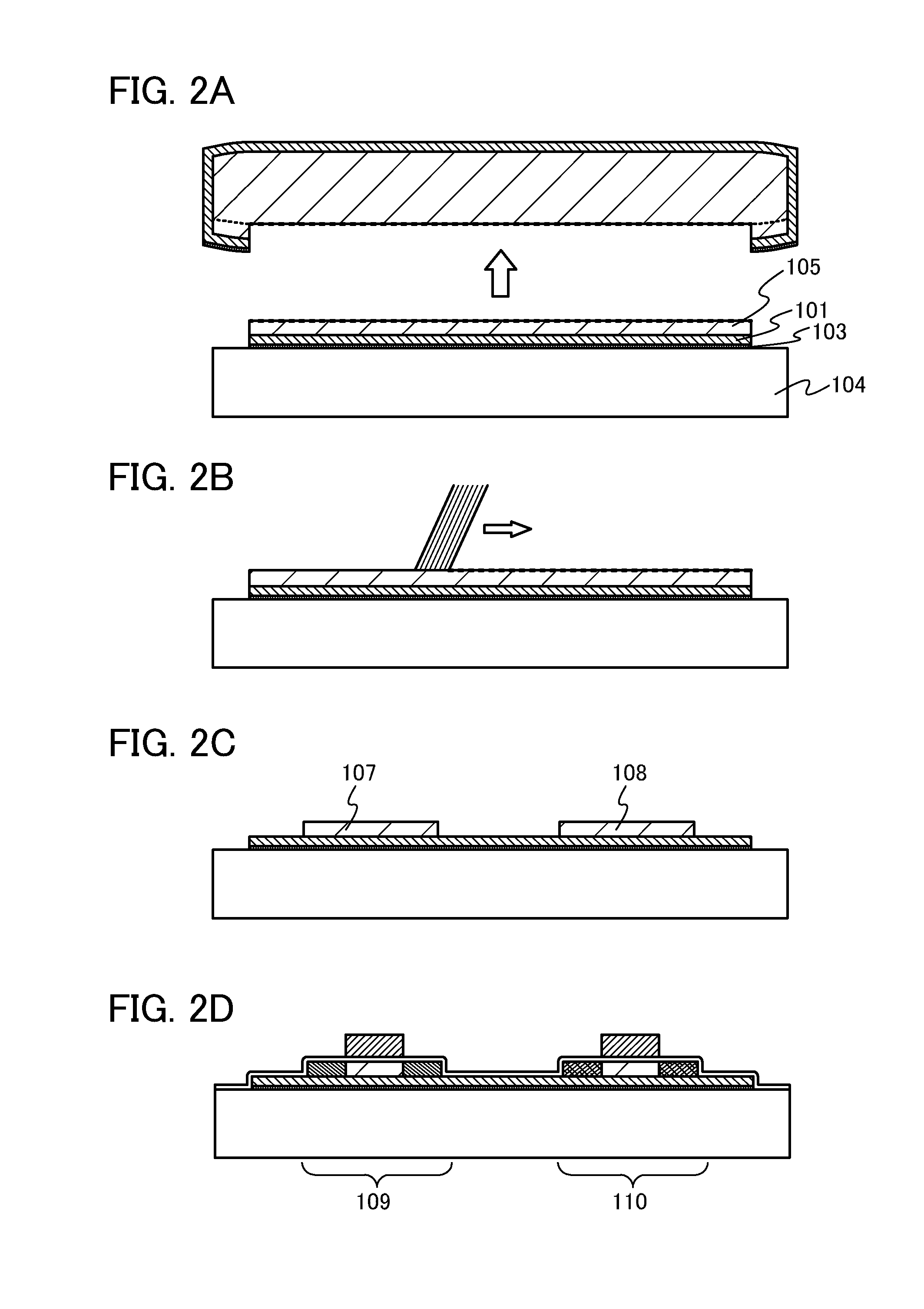
[0146]In this embodiment, a method for manufacturing a thin film transistor, one of semiconductor elements, will be described as an example of a method for manufacturing a semiconductor device using a base substrate to which a semiconductor film is attached, a so-called SOI substrate. By combining a plurality of thin film transistors, a variety of semiconductor devices can be formed.

[0147]First, as shown in FIG. 4A, an island-shape semiconductor film 602 and an island-shape semiconductor film 603 are formed over the base substrate 104 with the insulating film 103 and the oxide film 101 interposed therebetween.

[0148]In order to control threshold voltage, a p-type impurity such as boron, aluminum, or gallium or an n-type impurity such as phosphorus or arsenic may be added to the semiconductor films 602 and 603. For example, in the case of adding boron as an impurity imparting p-type conductivity, boron may be added at a concentration of 5×1016 cm−3 to 1×1017 cm−3 inclusive. The additi...


PUM

PropertyMeasurementUnit
Thicknessaaaaaaaaaa
Thicknessaaaaaaaaaa
Thicknessaaaaaaaaaa

Abstract

It is an object to provide a method for manufacturing an SOI substrate in which reduction in yield can be suppressed while impurity diffusion into a semiconductor film is suppressed. A semiconductor substrate provided with an oxide film is formed by thermally oxidizing the surface of the semiconductor substrate. Plasma is generated under an atmosphere of a gas containing nitrogen atoms and plasma nitridation is performed on part of the oxide film, so that a semiconductor substrate in which an insulating film containing nitrogen atoms is formed over the oxide film is obtained. After bonding the insulating film containing nitrogen atoms and a glass substrate to each other, the semiconductor substrate is split, whereby an SOI substrate in which the insulating film containing nitrogen atoms, the oxide film, a thin semiconductor film are stacked in this order is formed.

Description

BACKGROUND OF THE INVENTION[0001]1. Field of the Invention[0002]The present invention relates to a method for manufacturing a semiconductor device using a silicon-on-insulator (SOI) substrate.[0003]2. Description of the Related Art[0004]Demands for higher integration, higher operation speed, higher performance, and lower power consumption of a semiconductor integrated circuit have been more stringent, and in response to such demands, a transistor using an SOI substrate has attracted attention as an effective means that can take the place of a bulk transistor. Higher operation speed and lower power consumption of a semiconductor device can be expected more in the transistor using the SOI substrate than in the bulk transistor because a semiconductor film is formed over an insulating film in the transistor using the SOI substrate, and accordingly parasitic capacitance can be reduced and generation of leakage current flowing through the substrate can be suppressed. In addition, since th...

Claims


Application Information

Patent Timeline
IPC IPC(8): H01L21/762B23K26/00B23K26/352H01L21/02H01L21/265H01L21/322H01L21/336H01L27/12H01L29/786
CPCH01L21/02686H01L21/84H01L21/76254H01L27/1203
Inventor SHIMOMURA, AKIHISAKOYAMA, MASAKIHASEGAWA, TORU
Owner SEMICON ENERGY LAB CO LTD
Why Eureka
Try Eureka