Seed crystal for silicon carbide single crystal growth, method for producing the seed crystal, silicon carbide single crystal, and method for producing the single crystal

a silicon carbide and single crystal technology, applied in the direction of electric/magnetic/electromagnetic heating, instruments, transportation and packaging, etc., can solve the problems of in-crystal cavity defects, prone to porous carbon protective films, and in-crystal cavity defects, etc., to suppress crystal defects, high quality, and low crystal defect density

Inactive Publication Date: 2011-05-12
SHOWA DENKO KK
View PDF6 Cites 27 Cited by
  • Summary
  • Abstract
  • Description
  • Claims
  • Application Information

AI Technical Summary

Benefits of technology

[0035]According to the constitution described above, there can be provided a seed crystal for silicon carbide single crystal growth which is capable of suppressing crystal defects that arise from the interface between the seed crystal and the graphite, and producing a high quality silicon carbide single crystal having a low crystal defect density, with high reproducibility.
[0036]The seed crystal for silicon carbide single crystal growth of the invention has a constitution in which the seed crystal has a seed crystal formed of silicon carbide and having one surface defined as a growth surface for growing a silicon carbide single crystal by a sublimation method, and a carbon film formed on the surface of the opposite side of the growth surface of the seed crystal, wherein the film density of the carbon film is 1.2 g/cm3 to 3.3 g/cm3. Therefore, by increasing the strength of the carbon film, the carbon film can be made into a sufficiently hard film, and at the same time, can be made into a dense film having excellent gas barrier properties. The carbon film is preferably a non-crystalline carbon film having excellent gas barrier properties and having high adhesiveness to silicon carbide. Examples of the non-crystalline carbon film include a carbon film called DLC (diamond-like carbon) or a carbon film called glassy carbon, depending on the bonding state of carbon, but all of these have excellent gas barrier properties and high adhesiveness to silicon carbide due to their non-crystallinity. The representative density is such that the density of the DLC is about 1.2 g/cm3 to 3.3 g/cm3, and the density of the glassy carbon is about 1.2 g/cm3 to 3.3 g/cm3. By providing this dense protective film having high gas barrier properties and having high adhesiveness to silicon carbide on the rear surface of a seed crystal, crystal defects that arise from the interface between the seed crystal and graphite are suppressed, and a high quality silicon carbide single crystal having a low crystal defect density can be produced with good reproducibility.
[0037]The method for producing a seed crystal for silicon carbide single crystal grow

Problems solved by technology

This may cause the occurrence of in-crystal cavity defects such as micropipes.
This may cause the occurrence of the in-crystal cavity defects such as micropipes.
However, in the carbon protective film that is formed by carbonization (carbonization process) of SiC, which is mainly recommended in the PTL 1, Si-based volatile matter is generated at high temperatures so that the carbon protective film is prone to becoming porous, and sufficient gas barrier properties that are required to suppress the sublimation of the seed crystal cannot be obtained.
Accordingly, it is difficult to maintain the air-tightness at the contact parts between

Method used


Image

  • Seed crystal for silicon carbide single crystal growth, method for producing the seed crystal, silicon carbide single crystal, and method for producing the single crystal
  • Seed crystal for silicon carbide single crystal growth, method for producing the seed crystal, silicon carbide single crystal, and method for producing the single crystal
  • Seed crystal for silicon carbide single crystal growth, method for producing the seed crystal, silicon carbide single crystal, and method for producing the single crystal

Examples


embodiment 1

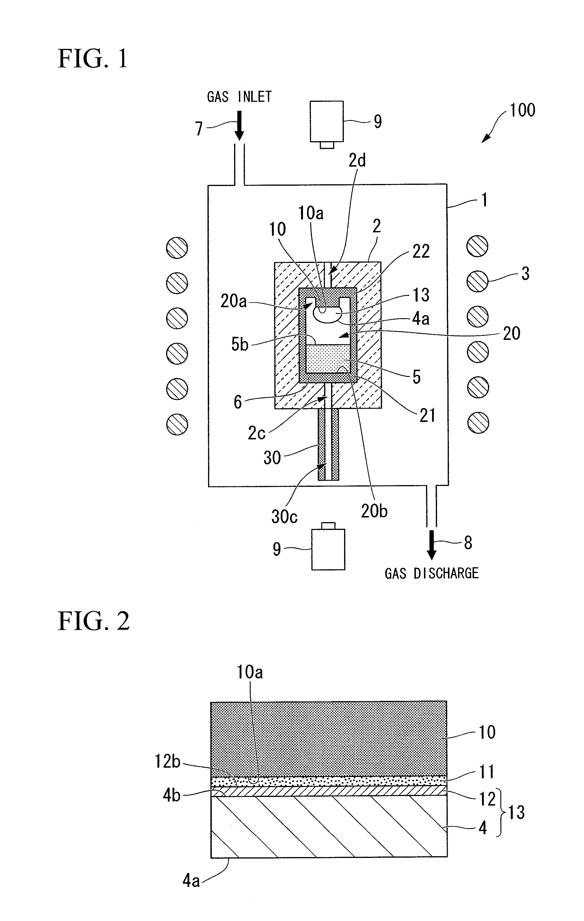
[0045]FIG. 1 is a diagram intended to explain an example of the seed crystal for silicon carbide single crystal growth, which is an embodiment of the invention, and is a schematic cross-sectional view showing an example of a crystal growing apparatus equipped with the seed crystal for silicon carbide single crystal growth which is an embodiment of the invention.

[0046]As shown in FIG. 1, the crystal growing apparatus 100 is approximately constructed to have a graphite crucible 6 covered with a thermally insulating material 2 disposed inside a vacuum container 1. The graphite crucible 6 includes a lid 22 and a body portion 21. In addition a seed crystal for silicon carbide single crystal growth 13, which is an embodiment of the invention, is bonded to one surface 10a of the protruded part 10 of the lid 22 of the graphite crucible 6.

[0047]As the material for the vacuum container 1, it is preferable to use a material that can maintain a high vacuum, and examples of the material include ...

example 1

[0121]First, a silicon carbide seed crystal substrate formed from a 4H-silicon carbide single crystal having a substrate area of about 1.5 cm2 and a thickness of 0.3 mm was provided, and this was subjected to washing with a sulfuric acid-hydrogen peroxide mixed solution at 110° C. for 10 minutes, to water washing with flowing ultrapure water for 5 minutes, to washing with an ammonia-hydrogen peroxide mixed solution for 10 minutes, to water washing with flowing ultrapure water for 5 minutes, to washing with a hydrochloric acid-hydrogen peroxide for 10 minutes, to water washing with flowing ultrapure water for 5 minutes, and to washing with a HF solution. Subsequently, the surface was oxidized at 1200° C., and then the surface was subjected again to HF washing.

[0122]Subsequently, a carbon film was formed on the (000-1) surface of this seed crystal substrate, and thus a seed crystal for silicon carbide single crystal growth was formed. A direct current discharge sputtering method was u...

example 2

[0137]A silicon carbide single crystal was formed in the same manner in Example 1, except that use was made of a seed crystal for growth formed from a silicon carbide single crystal having a thickness of 0.8 mm in which the (000-1) surface of a 4H-silicon carbide single crystal was defined as a growth surface and the (0001) surface as the surface of the side that was in contact with graphite, and a carbon film was formed on the (0001) surface.

[0138]The silicon carbide single crystal thus obtained was cut in parallel with the growth direction, and the cut surface was observed under a microscope. Similarly to the case of Example 1, almost no cavity-like defects were generated in the silicon carbide single crystal.

[0139]Thereby, it was confirmed that even in the case where the two surfaces of a seed crystal formed of silicon carbide have different polarities, the effect of suppressing defects was exhibited.


PUM

PropertyMeasurementUnit
Fractionaaaaaaaaaa
Thicknessaaaaaaaaaa
Thicknessaaaaaaaaaa

Abstract

A seed crystal for silicon carbide single crystal growth (13) which is attached to the lid of a graphite crucible charged with a raw material silicon carbide powder. The seed crystal includes a seed crystal (4) formed of silicon carbide having one surface defined as a growth surface (4a) for growing a silicon carbide single crystal by a sublimation method, and a carbon film (12) formed on the surface (4b) opposite to the growth surface of the seed crystal (4). Further, the film density of the carbon film (12) is 1.2 g/cm3 to 3.3 g/cm3.

Description

TECHNICAL FIELD [0001]The present invention relates to a seed crystal for silicon carbide single crystal growth, a method for producing the seed crystal, a silicon carbide single crystal, and a method for producing the single crystal.[0002]The present patent application claims priority from Japanese Patent Application No. 2008-176255 filed on Jul. 4, 2008, the disclosure of which is incorporated herein by reference.BACKGROUND ART [0003]Silicon carbide is a material having high thermal conductivity. Silicon carbide is also physically and chemically stable, has excellent thermal resistance and mechanical strength, and has high radiation resistance. Accordingly, silicon carbide is used as a material for rectifying elements or switching elements with high pressure resistance and low loss. Furthermore, silicon carbide has a broad energy band gap (forbidden band width), and a 4H type silicon carbide single crystal in particular has a forbidden band width of about 3 eV at room temperature....

Claims


Application Information

Patent Timeline
IPC IPC(8): C30B29/36B32B9/04B32B5/00C23C16/26C23C16/513C23C16/48C23C14/34C23C14/28C30B23/02
CPCC30B23/00C30B23/025Y10T428/265Y10T428/24273Y10T428/263C30B29/36
Inventor OYANAGI, NAOKIKOGOI, HISAO
Owner SHOWA DENKO KK
Why Eureka
Try Eureka