Multilayer film for encapsulating oxygen and/or moisture sensitive electronic devices

a technology of oxygen and/or moisture sensitive electronic devices, applied in the field of encapsulation technology, can solve the problems of destroying the transparency of the barrier substrate, affecting the performance of the electronic device, and the curing process is likely to damage the organic el layers

Active Publication Date: 2011-06-09
AGENCY FOR SCI TECH & RES
View PDF14 Cites 129 Cited by
  • Summary
  • Abstract
  • Description
  • Claims
  • Application Information

AI Technical Summary

Benefits of technology

[0011]The present inventors have found that “multilayer barrier films” (referred to herein also as “barrier films”) in which reactive nanoparticles are distributed in a polymeric binder to form one or more nanostructured (or nanoparticulate) layers are highly effectively for encapsulating moisture and oxygen sensitive devices. They are also useful for improving the gas barrier properties of existing barrier materials. Although moisture gettering nanoparticles have been used in barrier substrates, they have hitherto not been used as a coating or film. Conventional barrier substrates are capable of achieving low gas permeability with the use of metal or metal oxide barrier layers. However, it is found that metal and metal oxide layers gradually become opaque due to oxidation by permeating moisture and oxygen, thereby destroying the transparency of the barrier substrate. In order to avoid such a problem, attempts have been made to replace the metal or metal oxide barrier layer altogether in the barrier substrate. By avoiding the use of the metal or metal oxide film, and using a nanostructured layer containing reactive nanoparticles instead, the present invention overcomes the problem of the barrier substrate degenerating with use. In this regard, it is noted that the approach of using nanostructured layers as replacements for inorganic layer barrier substrates has so far been discouraged since the polymeric binder for holding the nanoparticles are cured through the application of a curing factor, such as ultraviolet light. As the organic electroluminescent (EL) layers of such devices are highly sensitive to ultraviolet light radiation, the curing process is likely to damage the organic EL layers. In conventional barrier substrates, such a problem does not occur as the ultraviolet light is prevented from reaching the device by the metal or metal oxide inorganic layers. In the absence of these inorganic layers, the EL layers are inevitably exposed to the ultraviolet light radiation. This problem is overcome in the present invention by combining the moisture and oxygen scavenging ability of the nanostructured layer(s) with the ultraviolet light shielding capability of the ultraviolet light neutralizing layer, to provide a purely “organic” barrier film in which inorganic metal and metal oxide layers found in conventional barrier substrates are omitted.
[0052]To facilitate transfers of a base substrate under vacuum or inert atmosphere from one chamber to another, a load lock system may be used. A conventional loadlock may be mounted to a gate valve attached to a main vacuum chamber. A substrate can then be easily moved into position through the large entry door onto the transfer stage in the loadlock chamber. After the loadlock is evacuated to the desired vacuum level, and the gate valve opened, the substrate is transferred into the process chamber through a magnet carriage along the main shaft of the loadlock. This allows repeated substrate loading and unloading without breaking vacuum in the main chamber. If vacuum chamber comprises a plurality of serially connected sub-chambers, the loadlock may comprise an extendable shaft movable through each individual sub-chamber.

Problems solved by technology

Although moisture gettering nanoparticles have been used in barrier substrates, they have hitherto not been used as a coating or film.
However, it is found that metal and metal oxide layers gradually become opaque due to oxidation by permeating moisture and oxygen, thereby destroying the transparency of the barrier substrate.
As the organic electroluminescent (EL) layers of such devices are highly sensitive to ultraviolet light radiation, the curing process is likely to damage the organic EL layers.

Method used


Image

  • Multilayer film for encapsulating oxygen and/or moisture sensitive electronic devices
  • Multilayer film for encapsulating oxygen and/or moisture sensitive electronic devices
  • Multilayer film for encapsulating oxygen and/or moisture sensitive electronic devices

Examples


example 1

Fabrication of an Encapsulated OLED

1. Surface Preparation of Substrates

[0094]Silicon oxide coated soda-lime glass substrates (display-quality glass) were cut into 50 mm×50 mm pieces and also any required sizes for use as a base or cover for the OLEDs. The pneumatically operated hollow die punch-cutting equipment or any conventional slitting machine could be used to slice the samples into the specified or required dimensions.

[0095]The water vapour permeation in the present encapsulation package may be mainly through the interface of the adhesive and substrate and also diffusion through adhesive sealing. The suitable surface pre-treatment process such as plasma treatment can eliminate the adhesion issues. Accordingly, they are rinsed with isopropyl alcohol (IPA) and blow-dried with nitrogen. These processes help to remove macro scale adsorbed particles on the surface. Acetone and methanol cleaning or rinsing is not recommended. After nitrogen blow-dry, the substrates are placed in th...

example 2

Encapsulation Vacuum Transfer Technique

[0107]The fabrication of the barrier film and the subsequent device encapsulation will be illustrated in the following for highly moisture or oxygen sensitive (up to a water permeation rate of 10−6 g / m2 / day level), organic devices fabricated on to rigid or plastic substrates, using either an on batch or roll to roll process:

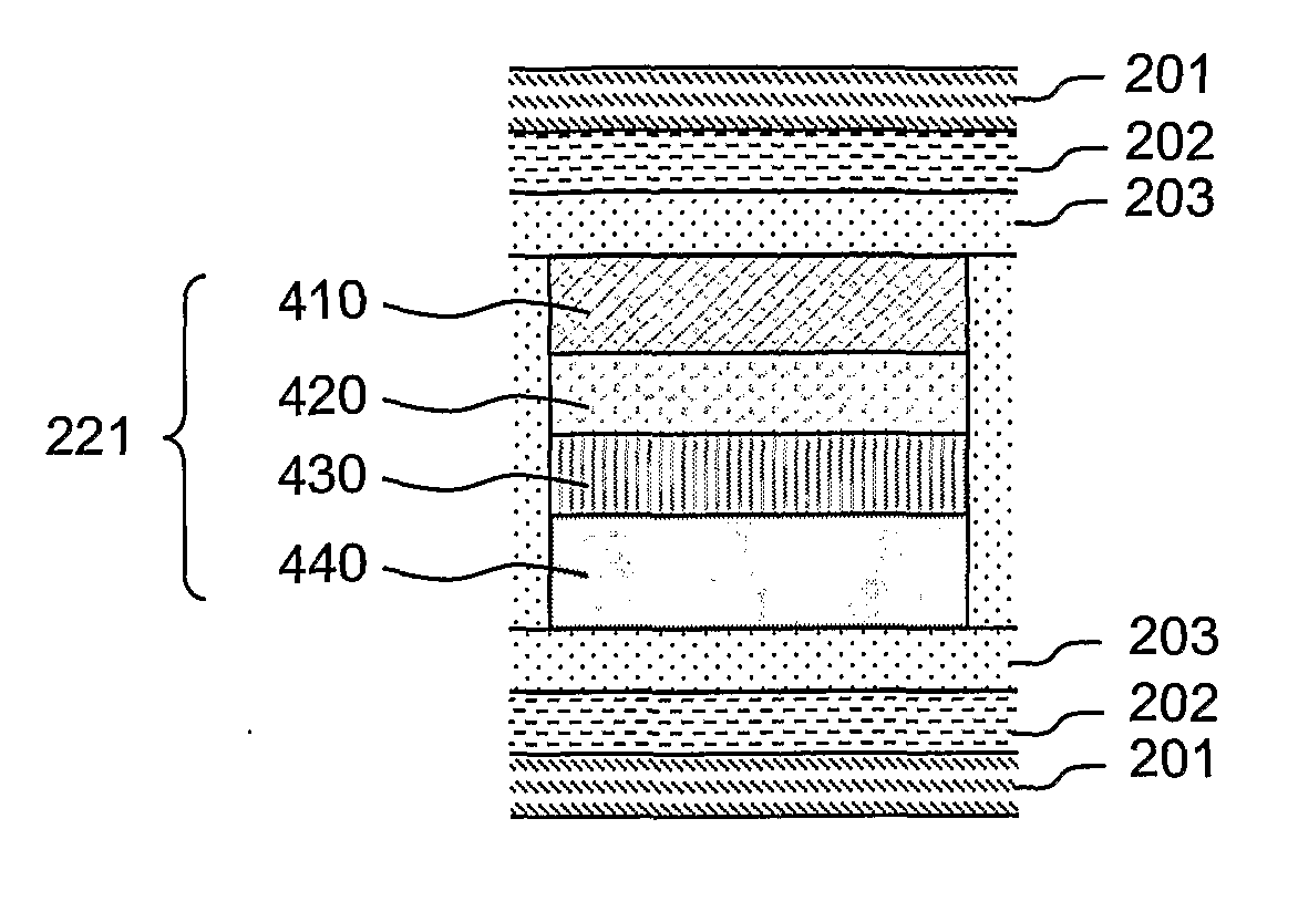
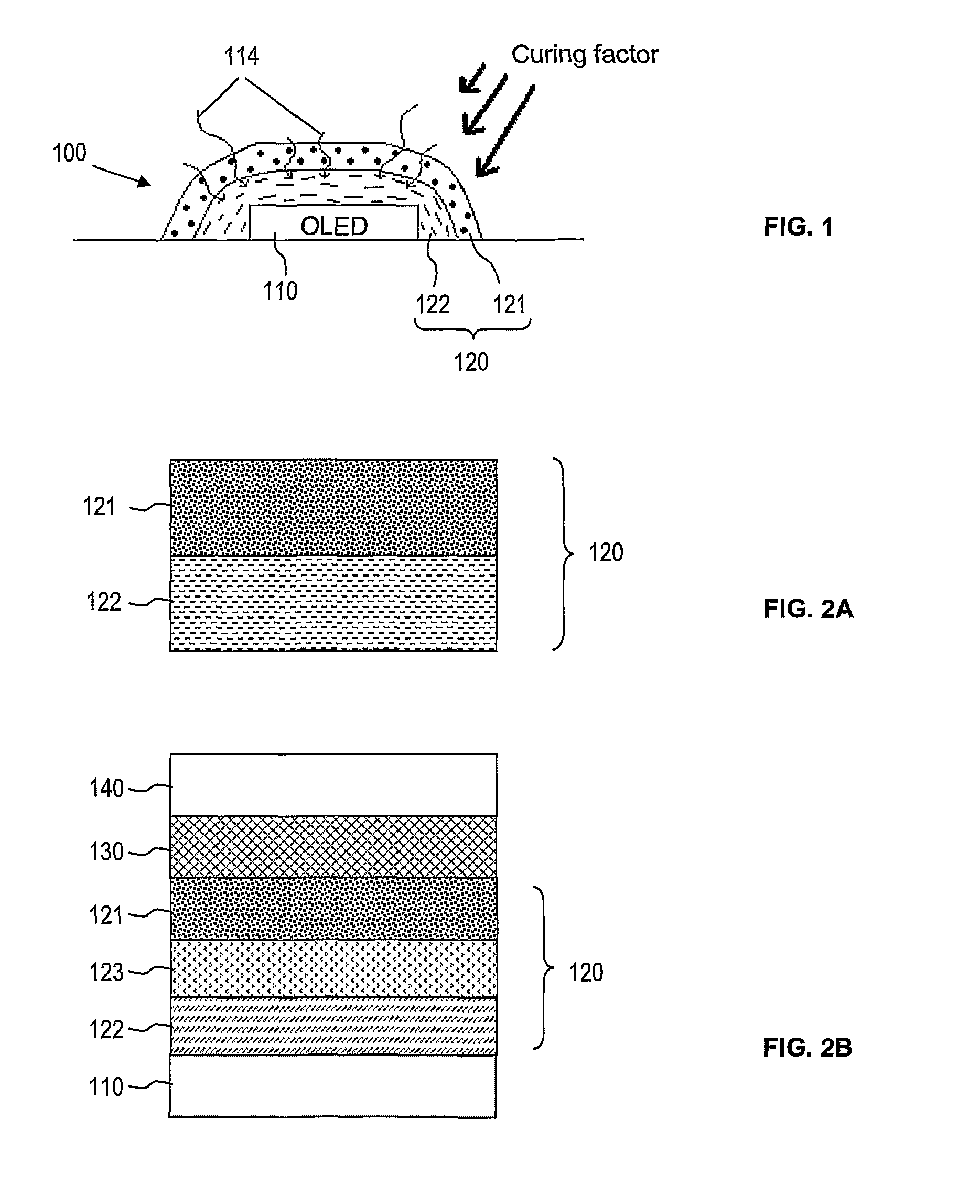
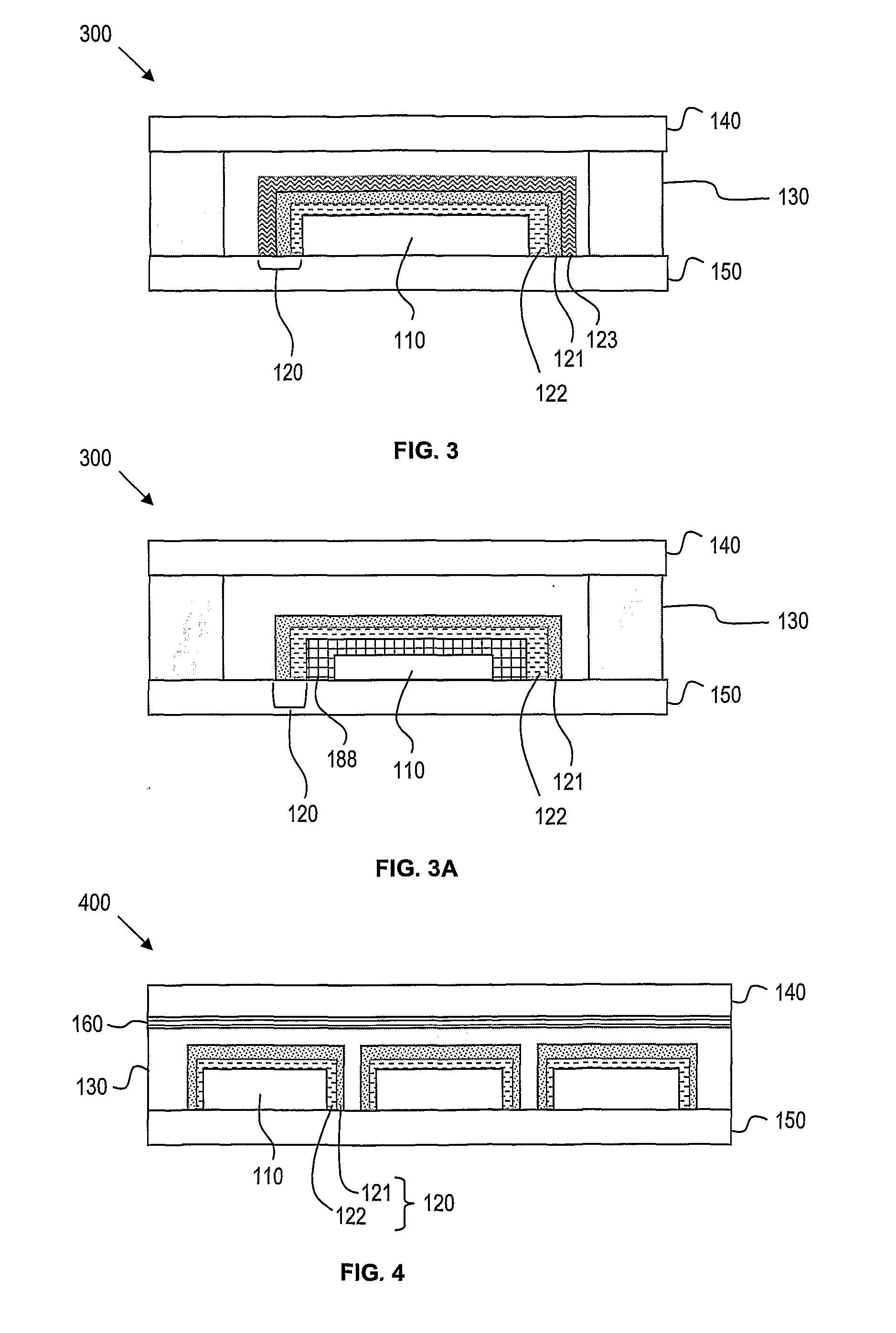
1. Device 110Organic Light Emitting Diode2. Solvent protection layerHigh refractive index solvent protectionoptical film (optional)3. Neutralizing layerTitanium oxide / Zinc Oxide rod structuredacrylic polymer4. Nanostructured layerReactive nanoparticles (other than titaniumoxide or zinc oxide, respectively) dispersedin acrylic polymer5. Cover substrateBarrier Plastic substrate / glass substrate

[0108]The device with the multi-layer barrier film of the invention that includes layers 3 and 4 will be adopted if cover substrates are fabricated on to plain plastic substrates. The solvent protection layer (film) 2 is only used optiona...


PUM

PropertyMeasurementUnit
particle sizesaaaaaaaaaa
lengthaaaaaaaaaa

Abstract

The present invention refers to a multilayer barrier film capable of encapsulating a moisture and / or oxygen sensitive electronic or optoelectronic device, the barrier film comprises at least one nanostructured layer comprising reactive nanoparticles capable of interacting with moisture and / or oxygen, the reactive nanoparticles being distributed within a polymeric binder, and at least one ultraviolet light neutralizing layer comprising a material capable of absorbing ultraviolet light, thereby limiting the transmission of ultraviolet light through the barrier film

Description

CROSS-REFERENCE TO RELATED APPLICATIONS[0001]This application claims benefit of priority of U.S. provisional application No. 61 / 043,534, filed Apr. 9, 2008, the contents of it being hereby incorporated by reference in its entirety for all purposes.FIELD OF THE INVENTION[0002]The present invention relates generally to encapsulation technology, more particularly to multilayer films for encapsulating oxygen and / or moisture sensitive electronic devices.BACKGROUND OF THE INVENTION[0003]In recent years, plastic electronics has grown in importance in an increasing number of areas, particularly in display applications used in a wide range of consumer handheld electronic devices containing miniaturised display screens. The goal of achieving an all-polymer electronics device has motivated research groups around the world to provide plastics—which are known for their low-cost processing, flexibility and toughness—with the electronic properties needed for practical circuitry in a wide range of ...

Claims


Application Information

Patent Timeline
Patent Type & Authority Applications(United States)
IPC IPC(8): H01L23/28H01L33/52H01L31/0203H01L21/56B32B27/06B32B27/20B05C15/00B82Y30/00
CPCH01L51/448H01L51/5237H01L51/5284H01L2251/5369Y10T428/25H05B33/10H01L51/524H01L51/56H05B33/04Y10T428/31504Y10T428/31721Y10T428/31938Y10T428/31931Y10T428/31725Y10T428/31935Y10T428/24995Y10T428/31511Y10T428/31507Y10T428/31663Y10T428/31551Y10T428/31533Y10T428/31678Y10T428/3154Y02E10/549H10K30/88H10K50/8445H10K50/846H10K50/841H10K50/865H10K2102/331B82B3/0004H10K50/84H10K71/00B32B27/20B82Y30/00B32B2457/206
Inventor RAMADAS, SENTHIL KUMARCHUA, SOO JINKE, LIN KAREN
Owner AGENCY FOR SCI TECH & RES
Why Eureka
Try Eureka