Modified graphene structures and methods of manufacture thereof

a graphene structure and graphene technology, applied in the field of modified graphene structure and methods of manufacture, can solve the problems of high defect density of chemically exfoliated graphene, inability to use chemically exfoliated graphene, and inability to achieve the effect of self-assembly and stabilisation of monolayers

Inactive Publication Date: 2012-03-08
UNIV COLLEGE CORK NAT UNIV OF IRELAND CORK +1
View PDF2 Cites 85 Cited by
  • Summary
  • Abstract
  • Description
  • Claims
  • Application Information

AI Technical Summary

Benefits of technology

[0013]an alkyl-chain spacer group (5) which separates the anchor group (4) and functional group (6) and facilitates the self-assembly and stabilisation of the monolayer (2).
[0058]Optionally, the method may involve the step of pre-treating the substrate prior to step (ii) with the functional organic molecule (3). In this preferred embodiment, the cleaned substrate (7) is then functionalised with a layer of functional organic molecules (3) such that the functional group (6A) binds to the substrate and the anchor groups (4A) are available to bind graphene (1) when this is deposited onto the substrate. In this manner, pre-treatment of the substrate, (for example silicon oxide substrates with amine-bearing molecules) greatly increases the observed number density of monolayer graphene flakes and also increases the mean size of deposited flakes.

Problems solved by technology

However, graphene is susceptible to adsorption of ambient matter (e.g. oxygen and water) which can introduce an inherent instability in graphene field effect devices.
The use of chemically exfoliated graphene is undesirable due to the high density of defects mentioned above.
Again, these chemically-derived sheets show a high defect density and have poor conductivity properties.
Thus, it is well known that graphene has many potential applications (e.g. field-effect devices) in many different fields, however, graphene is susceptible to adsorption of ambient matter (e.g. oxygen and water) which can introduce an inherent instability in graphene field effect devices.

Method used


Image

  • Modified graphene structures and methods of manufacture thereof
  • Modified graphene structures and methods of manufacture thereof
  • Modified graphene structures and methods of manufacture thereof

Examples


example 1

Graphene Deposition and Functionalisation

Materials

[0116]n-doped silicon wafers were purchased from SVM Silicon Valley Microelectronics Inc, USA. Polymer resist (Shipley S1813) and Microposit resist remover (R1165) were purchased from Chestech, UK.

[0117]Aqueous solutions of citrate-stabilised gold nanoparticles were purchased from British Biocell International. UK. Three separate families of nanoparticles with different core diameters (dNP) and concentrations (cNP) were employed for different functionalisation experiments:

dNP=30 nm, cNP=2.0×10¹¹ nanoparticles / mL

dNP=20 nm, cNP=7.0×10¹¹ nanoparticles / mL

dNP=10 nm, cNP=5.7×10¹² nanoparticles / mL

[0118]1,10-diaminodecane, 1-aminodecane, 1-aminohexane, methanol and tetrahydrofuran were purchased from Sigma-Aldrich, UK.

Full Method Protocol

1. Substrate Preparation and Cleaning

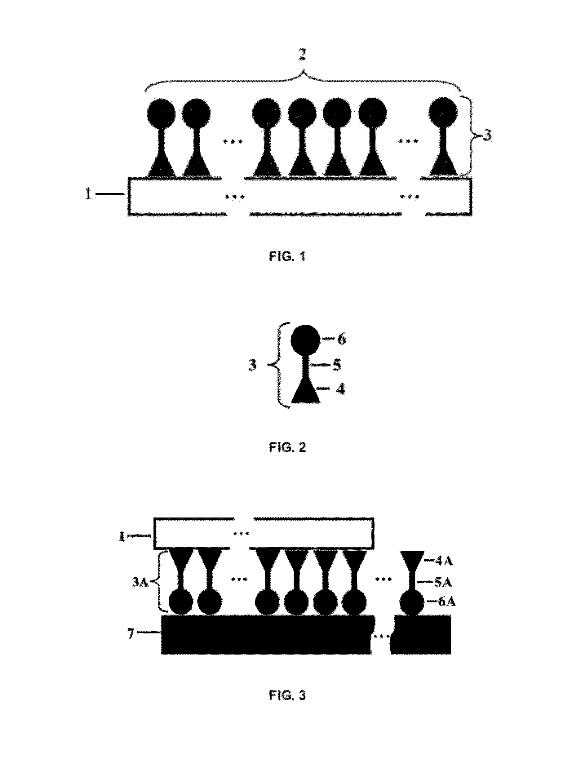
[0119]90 nm of silicon oxide was thermally grown on commercial n-doped silicon wafers using dry oxidation. The rear surface of the wafer was stripped of the oxide to enab...

example 2

Functionalisation of Graphene with Gold Nanoparticles

[0135]Silicon oxide chips bearing graphene sheets, where the top surface of graphene was functionalised with 1,10-diaminodecane made in accordance with Example 1 were immersed in a solution of citrate-stabilised gold nanoparticles (30 nm core diameter) for 6 hours. The chip was then removed and rinsed in ultra pure water before drying under a stream of nitrogen. Scanning electron microscopy (JEOL 6700F, 10 kV beam voltage) was employed to image and record the number density of nanoparticles present at the surfaces of these functionalised monolayer graphene sheets.

[0136]FIG. 11 shows a schematic of process for the functionalisation of graphene: (a) Graphene (1) on substrate (7); (b) functionalised with a layer of molecules (2) that can (c) bind gold nanoparticles (11).

Results

[0137]FIG. 11(d) is a scanning electron microscope image showing a high surface density of citrate-stabilised gold nanoparticles (30 nm core diameter) bound to...

example 3

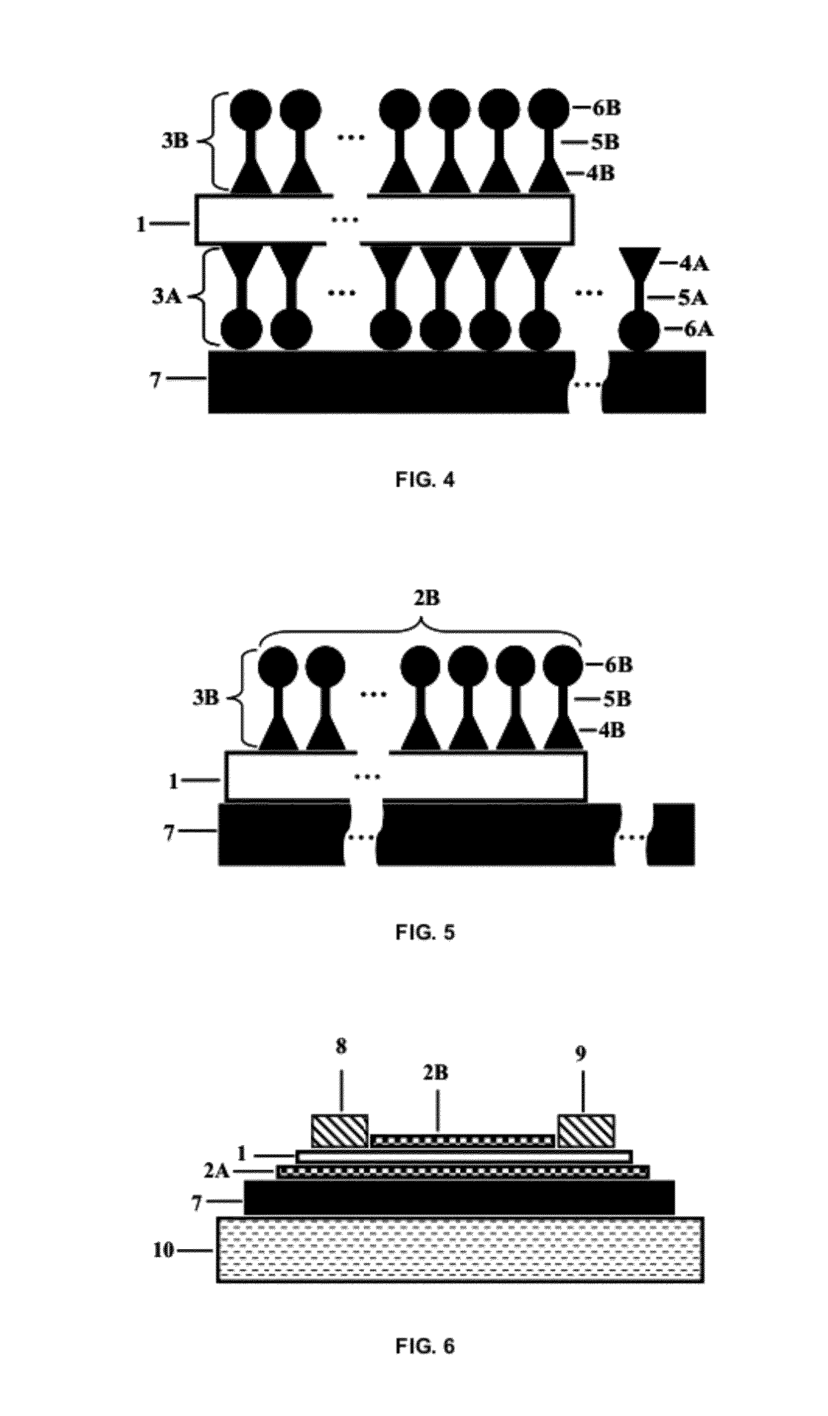
Preparation of Graphene Field Effect Devices

[0140]A number of field effect devices were fabricated and measured as shown in FIGS. 12(a), (c), and (e).[0141]FIG. 12(a) is a field-effect device comprising a graphene layer (1) deposited on a clean thermally-grown layer of silicon oxide (7) on a doped silicon substrate (10). The silicon substrate acts as a back-gate electrode for the device.[0142]FIG. 12(c) is a schematic of the same graphene field effect device following annealing in vacuum.[0143]FIG. 12(e) is a schematic the same graphene field effect device following adsorption of a layer of functional molecules onto the graphene by immersion in a solution of 1,10-diaminodecane in methanol-tetrahydrofuran.

Field Effect Device (FIG. 12(a))

[0144]a. Graphene sheets deposited on oxidised silicon chips were electrically contacted with nickel electrodes using standard optical lithography, metal deposition and lift-off procedures.

[0145]After the deposition of the graphene by mechanical exfol...


PUM

PropertyMeasurementUnit
binding energyaaaaaaaaaa
thicknessaaaaaaaaaa
length/widthaaaaaaaaaa

Abstract

The present invention is directed to a modified graphene structure comprising at least one graphene sheet (1) and a self-assembled monolayer (2) of functional organic molecules (3) non-covalently bonded to the top and / or bottom basal planes of the graphene sheet and methods of manufacture thereof. The present invention is also directed to devices comprising the modified graphene structures, including but not limited to field-effect devices and biosensors, and to methods using the modified graphene structures.

Description

FIELD OF THE INVENTION[0001]The present invention is directed to a modified graphene structure and methods of manufacture thereof. The present invention is also directed to devices comprising the modified graphene structures, including but not limited to field-effect devices and biosensors and methods using the modified graphene structures.BACKGROUND TO THE INVENTION[0002]Monolayer graphene is a single layer of carbon atoms arranged in a two-dimensional (2D) honeycomb-like lattice, and is a basic building block for carbon materials of other dimensionalities, including fullerenes, nanotubes, few-layer graphene 10 layers) or 3D graphite.[0003]In 2004 a method for the micromechanical exfoliation of few-layer graphene from graphite and fabrication of back-gated graphene field-effect devices was reported (Novoselov et al., “Electric field effect in atomically thin carbon films”Science, 2004, 306, 666). Methods for large area preparation of graphene have also been reported including therm...

Claims


Application Information

Patent Timeline
Patent Type & Authority Applications(United States)
IPC IPC(8): B32B9/04G01N31/00B32B19/00G01N33/53
CPCB82Y10/00G01N27/4146H01L29/66742H01L51/0545H01L29/78684H01L51/0045H01L29/78603H10K85/20H10K10/466
Inventor LONG, BRENDAMANNING, MARYSZAFRANEK, BARTHOLOMAUSQUINN, AIDAN
Owner UNIV COLLEGE CORK NAT UNIV OF IRELAND CORK
Why Eureka
Try Eureka