Naphthalene derivative, resist bottom layer material, and patterning process

a bottom layer material and etching technology, applied in the field of naphthalene derivatives, can solve the problems of increasing surface roughness after etching to a serious concern, weak resistance of acrylate to substrate etching, and approaching the essential limit of resolution determined by the light source wavelength, etc., to achieve improved etching resistance, high heat resistance, and solvent resistance

Active Publication Date: 2012-03-15
SHIN ETSU CHEM IND CO LTD
View PDF14 Cites 61 Cited by
  • Summary
  • Abstract
  • Description
  • Claims
  • Application Information

AI Technical Summary

Benefits of technology

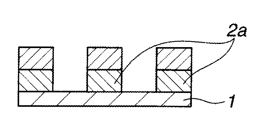
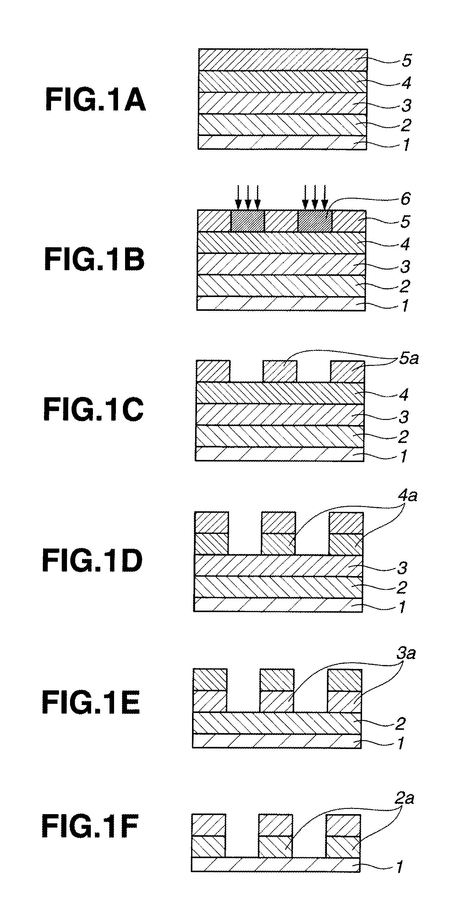
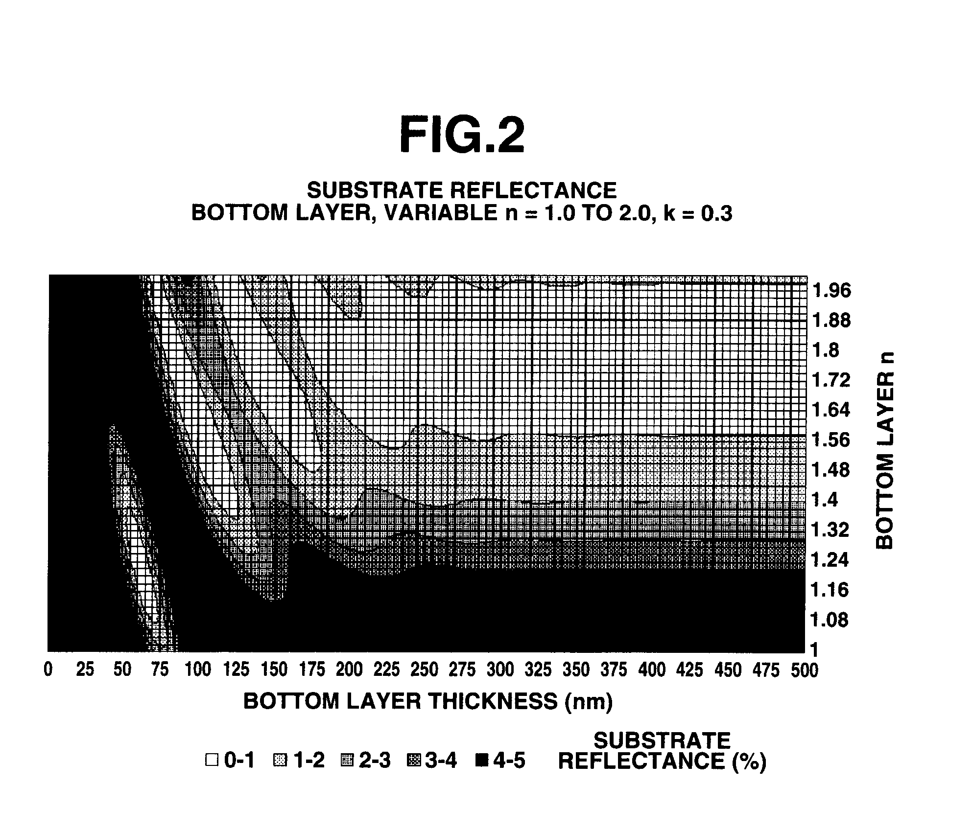
[0066]Since the method for forming a resist bottom layer which is included in a multilayer resist film of at least three layers used in the lithography uses a resist bottom layer material comprising a naphthalene derivative having formula (1) or (2) or a polymer comprising recurring units of the naphthalene derivative, the resulting resist bottom layer has values of n and k optimum as ARC film, burying properties, improved etch resistance, high heat resistance and solvent resistance, capable of minimizing outgassing during bake, and being devoid of twist during etching of an underlying substrate through a line pattern having a high aspect ratio and a width of less than 60 nm. When an inorganic hard mask is formed by CVD on the resist bottom layer which has been formed by a spin coating technique, the resist bottom layer has sufficient heat resistance to withstand the temperature treatment for forming the inorganic hard mask middle layer. A pattern forming process in which the resist bottom layer formed by spin coating is combined with the inorganic hard mask formed by CVD is available.

Problems solved by technology

While a number of recent efforts are being made to achieve a finer pattern rule in the drive for higher integration and operating speeds in LSI devices, the commonly used light exposure lithography is approaching the essential limit of resolution determined by the light source wavelength.
However, the resistance of the acrylate to substrate etching is weak as compared with polyhydroxystyrene, and a considerable proportion of the acrylate must be copolymerized in order to reduce the k value.
Through copolymerization of acrylate, the surface roughness after etching is increased to a level of serious concern.
The resist bottom layer is too thick to utilize the optical interference effect and lacks the anti-reflective function due to the offsetting effect by optical interference.
When an amorphous carbon bottom layer is formed by CVD using a reactant gas such as methane, ethane or acetylene gas, it is difficult to bury steps to be flat.
However, the upper limit of the temperature to which the wafer can be heated by the lithography wafer process is up to 600° C., preferably up to 500° C. when thermal impacts like device damage and wafer deformation are taken into account.
However, the CVD has poor step burying properties as pointed out above, and the CVD apparatus may be difficult to introduce because of its price and footprint area.
In the event the processable substrate is a low-dielectric-constant film, the photoresist may be poisoned therefrom (poisoning problem).
Because of the problem of film slimming or resin degradation after heating due to shortage of heat resistance, heat treatment of a resist bottom layer material is usually carried out at or below 300° C., typically 80 to 300° C. The heat treated film, however, still suffers from slimming after solvent treatment or twisting of the pattern during etching of the substrate.

Method used


Image

  • Naphthalene derivative, resist bottom layer material, and patterning process
  • Naphthalene derivative, resist bottom layer material, and patterning process
  • Naphthalene derivative, resist bottom layer material, and patterning process

Examples


synthesis example 1

Synthesis of Naphthalene Derivative (I)

[0144]

(1-1)

[0145]A three-neck flask was charged with 15.9 g (5.6 mmol) of 1,1′-bi-2,2′-naphthol, 10.0 g (5.6 mmol) of 9-fluorenone, and 125 ml of 1,2-dichloroethane, which were dissolved by keeping the flask in an oil bath. After dissolution was confirmed, 0.3 ml of 3-mercaptopropionic acid and 3.0 ml of methanesulfonic acid were added dropwise. Under reflux, reaction was effected for 10 hours. At the end of reaction, the reaction solution was diluted with 300 ml of ethyl acetate, and transferred to a separatory funnel where it was washed with water and separated. Water washing was repeated until the water layer became neutral. The organic layer was concentrated under reduced pressure, and 100 ml of tetrahydrofuran (THF) was added to the residue, which was poured to 1,300 ml of hexane, allowing the polymer to crystallize. The crystallized polymer was collected by filtration and dried in vacuum, obtaining naphthalene derivative (I).

Naphthalene D...

synthesis example 2

Synthesis of Naphthalene Derivative (II)

[0152]

In the formulae, x and y each indicate a proportion of the corresponding partial structure.

(1-2)

[0153]A three-neck flask was charged with 7.9 g (2.8 mmol) of 1,1′-bi-2,2′-naphthol, 7.5 g (2.8 mmol) of 2,2′-dinaphthyl ether, 10.0 g (5.6 mmol) of 9-fluorenone, and 60 ml of 1,2-dichioroethane, which were dissolved by keeping the flask in an oil bath. After dissolution was confirmed, 0.3 ml of 3-mercaptopropionic acid and 3.0 ml of methanesulfonic acid were added dropwise. Under reflux, reaction was effected for 11 hours. At the end of reaction, the reaction solution was diluted with 100 ml of methyl isobutyl ketone and 100 ml of toluene, and transferred to a separatory funnel where it was washed with water and separated. Water washing was repeated until the water layer became neutral. The organic layer was concentrated under reduced pressure, and 140 ml of THF was added to the residue, which was poured to 1,500 ml of hexane, allowing the po...

synthesis example 3

Synthesis of Naphthalene Derivative (III)

[0160]

(1-3)

[0161]A three-neck flask was charged with 24.87 g (86.8 mmol) of 1,1′-bi-2,2′-naphthol, 20.0 g (86.8 mmol) of 9-benzo[b]fluorenone, and 120 ml of 1,2-dichioroethane, which were dissolved by keeping the flask in an oil bath. After dissolution was confirmed, 0.60 ml of 3-mercaptopropionic acid and 6.0 ml of methanesulfonic acid were added dropwise. Under reflux, reaction was effected for 14 hours. At the end of reaction, the reaction solution was diluted with 500 ml of ethyl acetate, and transferred to a separatory funnel where it was washed with water and separated. Water washing was repeated until the water layer became neutral. The organic layer was concentrated under reduced pressure, and 200 ml of THF was added to the residue, which was poured to 1,500 ml of hexane, allowing the polymer to crystallize. The crystallized polymer was collected by filtration and dried in vacuum, obtaining naphthalene derivative (III).

Naphthalene Der...


PUM


Abstract

A naphthalene derivative having formula (1) is provided wherein An and Art denote a benzene or naphthalene ring, and n is such a natural number as to provide a weight average molecular weight of up to 100,000. A material comprising the naphthalene derivative or a polymer comprising the naphthalene derivative is spin coated to form a resist bottom layer having improved properties. A pattern forming process in which a resist bottom layer formed by spin coating is combined with an inorganic hard mask formed by CVD is available.

Description

CROSS-REFERENCE TO RELATED APPLICATION[0001]This non-provisional application claims priority under 35 U.S.C. §119(a) on Patent Application No. 2010-202660 filed in Japan on Sep. 10, 2010, the entire contents of which are hereby incorporated by reference.TECHNICAL FIELD[0002]This invention relates to a naphthalene derivative and a method for preparing the same. It also relates to a resist bottom layer material for forming a resist bottom layer useful as an antireflective coating (ARC) in the multilayer resist process used in micropatterning for the fabrication of semiconductor devices or the like, a method for forming a resist bottom layer, and a pattern forming process adapted for the lithography including exposure to KrF excimer laser (248 nm), ArF excimer laser (193 nm), F2 laser (157 nm), Kr2 laser (146 nm), Ar2e laser (126 nm), soft X-ray or EUV (13.5 nm), electron beam, or X-ray, using the resist bottom layer material.BACKGROUND ART[0003]While a number of recent efforts are bei...

Claims


Application Information

Patent Timeline
Patent Type & Authority Applications(United States)
IPC IPC(8): H01L21/311C08G8/02G03F7/004H01L21/31
CPCG03F7/091B05D1/40G03F7/20C08G61/10G03F7/00B05D3/007C07C37/16C07C39/17C08G61/02G03F7/038
Inventor KINSHO, TAKESHIKORI, DAISUKETAKEMURA, KATSUYAWATANABE, TAKERUOGIHARA, TSUTOMU
Owner SHIN ETSU CHEM IND CO LTD
Why Eureka
Try Eureka