[0017]The present invention augments methods for making structures, including nanosized and microsized thin film structures that exhibit a high degree of smoothness useful for applications in
microelectronics. Deposition processes of the invention utilize
smoothing agents capable of selectively adjusting the relative rates of processes involved in thin film formation and growth to access enhanced
nucleation densities resulting in smooth thin film structures, including ultrathin (e.g., <10 nm) smooth films. The invention provides methods for conformally coating and / or filling features of a substrate with a film, including high aspect ratio (e.g. aspect ratio >10) recessed features such as trench and / or via structures having nanosized vertical (e.g. depth) and / or lateral (e.g., width and length) dimensions. In an embodiment, for example, the present methods are useful for making thin films having a low
surface roughness such as a root mean squared (rms)
surface roughness less than or equal to 1 nm. In an embodiment, for example, the present methods enable formation of smooth thin film structures exhibiting substantially uniform densities (e.g., within 20%) that are substantially free of pinholes or other gaps (e.g., having a volume of void per area of film less than or equal to 1×10⁻⁶ μm3 / μm2, or 1×10⁻⁶ μm) in the bulk or interface of the thin film and a device substrate. The present methods are compatible with a wide range of existing materials, processing techniques and processing conditions, and, thus, provide a versatile processing platform for making diverse classes of device structures, including
diffusion barriers,
dielectric layers and metallic
layers, such as
electrical contacts and interconnects. Methods of the present invention are useful for fabricating a range of functional electronic devices including integrated electronic circuits, macroelectronic devices and arrays, memory devices, display devices, sensors, MEMS & NEMS systems, photovoltaic devices, and micro- and nanofluidic systems.
[0022]In aspect, the
smoothing agent is an inhibitor gas. In an embodiment, for example,
accommodation of the smoothing agent by the nuclei, the substrate or both the nuclei and the substrate decreases the growth rate of the nuclei sufficiently such that growth and coalescence of nuclei, including additional nuclei, on the substrate generates the smooth layer. In an embodiment, for example,
accommodation of the smoothing agent by the nuclei, the substrate or both the nuclei and the substrate decreases the growth rate of the nuclei by a factor of at least 2 relative to a growth rate of the nuclei in the absence of the smoothing agent. In an embodiment, for example,
accommodation of the smoothing agent by the nuclei, the substrate or both the nuclei and the substrate decreases the growth rate of the nuclei by a factor selected over the range of 2 to 100 relative to a growth rate of the nuclei in the absence of the smoothing agent. In an embodiment, for example, the precursor gas has a net
sticking coefficient with respect to accommodation on the nuclei, wherein accommodation of the smoothing agent by the nuclei, the substrate or both the nuclei and the substrate results in a decrease of the net sticking coefficient of the precursor gas with respect to accommodation on the nuclei by a factor greater than or equal to 2. In an embodiment, for example, the precursor gas has a net sticking coefficient with respect to accommodation on the nuclei, wherein accommodation of the smoothing agent by the nuclei, the substrate or both the nuclei and the substrate results in a decrease of the net sticking coefficient of the precursor gas with respect to accommodation on the nuclei by a factor selected from the range of 2 to 1000, and optionally selected from the range of 2 to 100, and optionally selected from the range of 2 to 10.
[0024]An
advantage of the present methods is the ability to generate high quality smooth and ultrathin film structures, for example, thin films having thicknesses less than or equal to 100 nanometers, optionally less than or equal to 20 nanometers, optionally less than 10 nanometers, and optionally less than 5 nanometers. In an embodiment, for example, the ultrathin smooth layer generated by the present methods has a thickness selected over the range of 0.3 nm to 20 nm. An
advantage of the present methods is the ability to generate high quality ultrasmooth film structures, for example, having a
surface roughness (rms) less than or equal to 20 nm, optionally a surface roughness (rms) less than or equal to 10 nm, and optionally a surface roughness (rms) less than or equal to 5 nm. In an embodiment, for example, the smooth layer generated by the present methods has a surface roughness (rms) selected over the range of 0.1 nm to 10 nm, and optionally a surface roughness (rms) selected over the range of 0.1 nm to 2 nm.
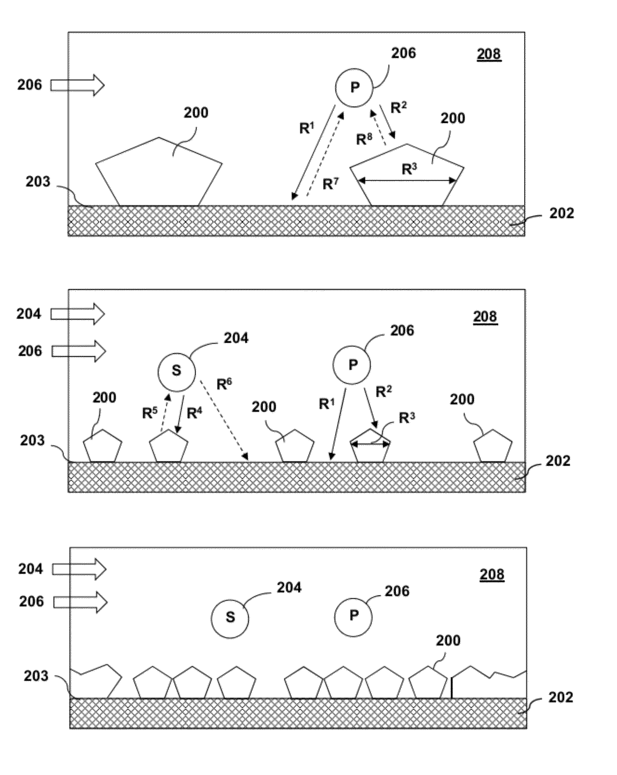
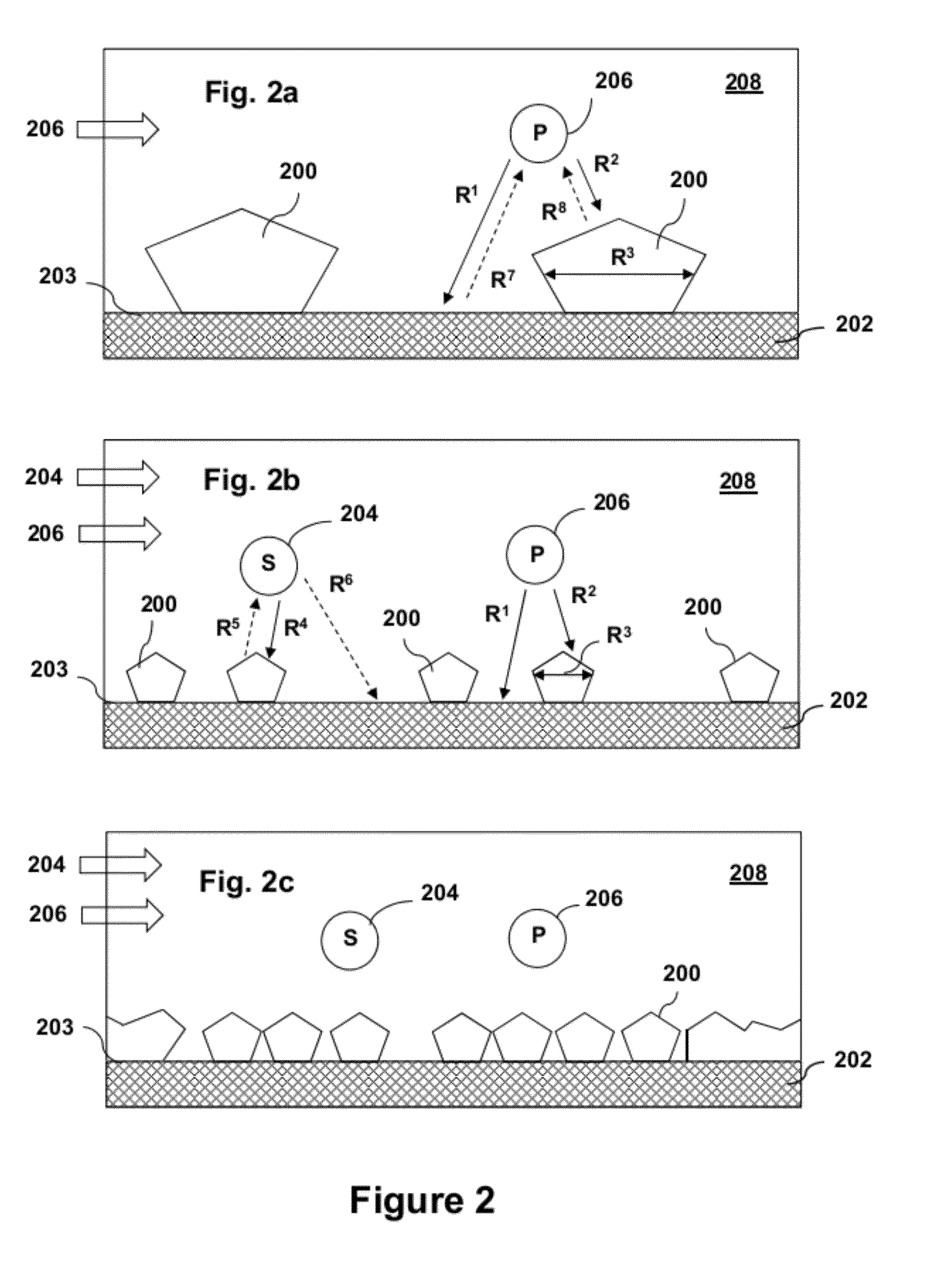
[0025]Use of a smoothing agent comprising an inhibitor gas is beneficial in some methods of the present invention for selectively adjusting the relative rates of processes involved in the
nucleation, growth and coalescence of deposited materials, such as
chemical vapor deposition and
atomic layer deposition materials. In some aspects, for example, processing using an inhibitor gas provides control over the relative rates of formation and growth of nuclei on a
substrate surface so as to access deposition conditions resulting in the formation of a smooth conformal layer, such as a smooth conformal thin film.
[0027]In some embodiments, for example, smoothing agent is accommodated by surfaces of the growing nuclei, thereby generating condensed phase species on, or within, the nuclei that decrease the
rate of growth of the nuclei, for example, by decreasing the rate of accommodation of precursor gases by surfaces of the nuclei. In some embodiments, for example, interaction between the smoothing agent and the surfaces of the nuclei results in formation of condensed phase species on the surface and / or within the nuclei, such as species physisorbed on the surface of the nuclei, species chemisorbed on the surface of the nuclei and species on the surface of the nuclei that are products of reaction(s) of the smoothing agent and nuclei and / or
decomposition of the smoothing agent. Such condensed phase species include condensed phase inhibitor species including stable species present on the surface of the nuclei and metastable species that undergo reaction and / or subsequent release to the
gas phase. In some embodiments, processes of accommodation of the smoothing agent by the surfaces of the nuclei and loss of condensed phase species from the surfaces of the nuclei establish a
steady state amount of condensed phase species on the nuclei, for example, a
steady state amount of condensed phase species providing a decrease in the of
rate of growth of nuclei relative to the rate of generation of new nuclei so as to generate a smooth layer on the substrate. In some embodiments, the presence of condensed phase species on the surface and / or in the bulk of nuclei function to increase the rates of chemical reactions resulting in reformation and subsequent
desorption of precursor.
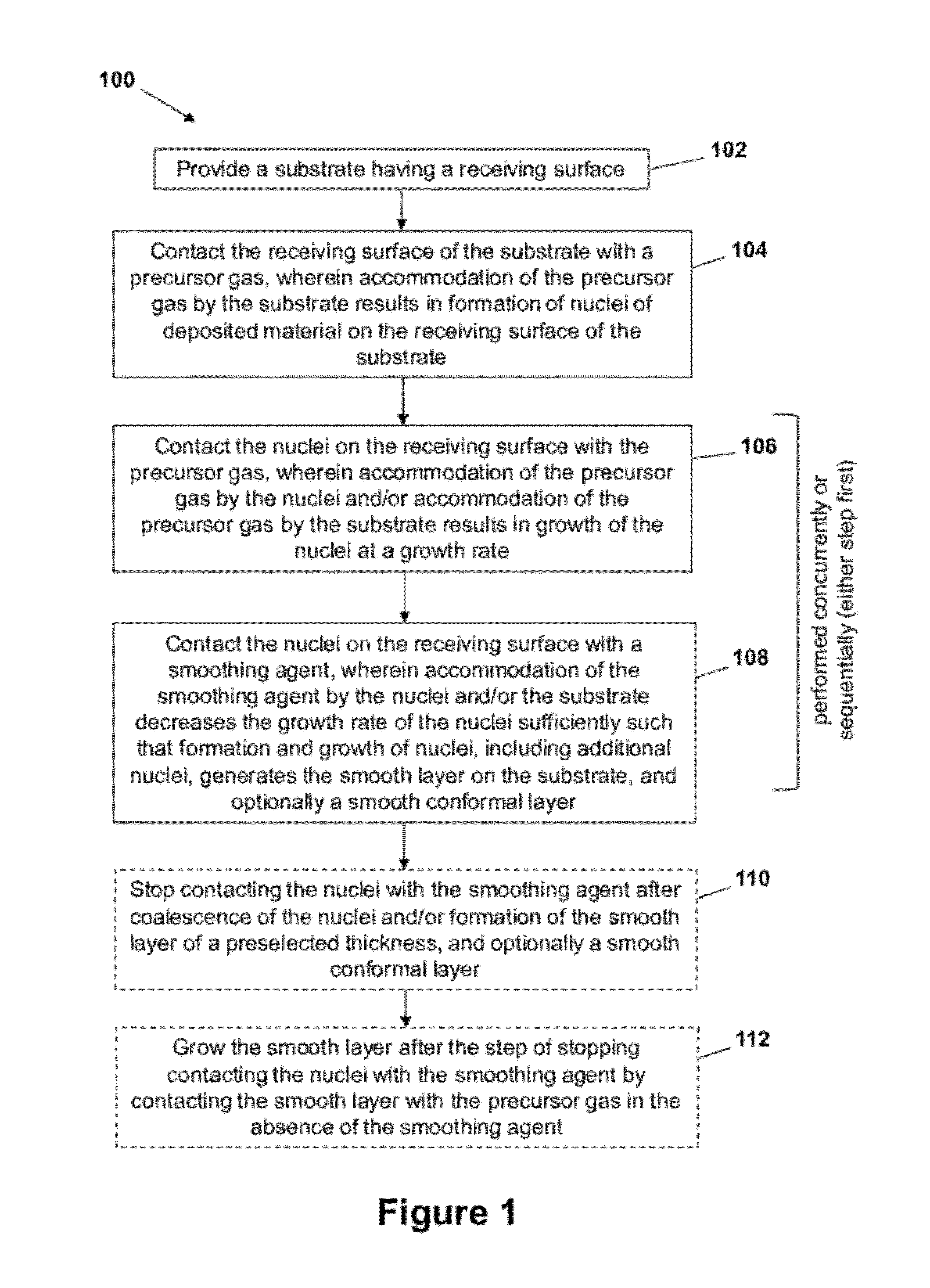
[0041]In an aspect, the invention provides a method of enhancing a nucleation density of a thin film deposited on a substrate, the method comprising the steps of: (1) providing the substrate having a receiving surface; (2) contacting the receiving surface of the substrate with a precursor gas, wherein accommodation of the precursor gas by the substrate results in formation of nuclei of deposited material on the receiving surface of the substrate; (3) contacting the nuclei on the receiving surface with the precursor gas; wherein accommodation of the precursor gas by the nuclei, substrate or both the nuclei and the substrate results in growth of the nuclei at a growth rate; and (4) contacting the nuclei, the substrate or both the nuclei and the substrate with a smoothing agent, wherein accommodation of the smoothing agent by the nuclei, the substrate or both the nuclei and the substrate results in enhancement of the nucleation density of the thin film deposited on the substrate. In an embodiment, for example, the nucleation density of the thin film is greater than or equal to 1×1011 cm−2. In an embodiment, for example, the thin film coalesces at a thickness less than or equal to 5 nm and optionally less than or equal to 1 nm and optionally less than or equal to 0.5 nm. In an aspect, the nucleation density of the thin film is enhanced relative to equivalent deposition conditions but in the absence of smoothing agent, for example, enhanced by a factor of at least 2 and optionally enhanced by a factor of at least 100.

