Mram etching processes

a technology of etching process and memory element, which is applied in the manufacture/treatment of electrical apparatus, semiconductor devices, and galvano-magnetic devices. it can solve the problems of slow etching, generate uniformity problems, and passivation of the surface of the top electrode by the hard mask etchant, and achieve low etching rate, good selectivity, and high selectivity.

Active Publication Date: 2013-02-28
AVALANCHE TECH
View PDF9 Cites 23 Cited by
  • Summary
  • Abstract
  • Description
  • Claims
  • Application Information

AI Technical Summary

Benefits of technology

[0013]The second embodiment uses a multilayered etching hard mask including a layer having a good selectivity (low etch rate) in an ambient used for top electrode or hard mask etching. A conventional hard mask layer material such as silicon oxide, silicon nitride, titanium nitride and their substitutes is selected for the first hard mask layer. The second hard mask layer is preferably a material having a slow etching rate in the hard mask or top electrode etching ambient such as a carbon fluoride system. Preferred materials include a borazinic film, aluminum oxide, copper, and aluminum, which have high selectivity compared to silicon oxide in the selected etching system. This embodiment works with Ta as a top electrode material. The second hard mask pad helps the Ta etching process by maintaining the thickness of the first hard mask pad. As a further benefit, the straight sidewall profile of the first hard mask pad and electrode is maintained since the selectivity of the second hard mask is good.
[0014]The third embodiment uses a multilayered top electrode structure including a first Cu layer under a second layer such as Ta. Using the Ta / Cu embodiment compensates for high etch rate of Cu in the MTJ etching ambient. In this embodiment the total top electrode thickness is increased to widen a process window of the bitline interconnection process. As an option, a passivation layer may be deposited after the bottom electrode has been etched to prevent MTJ from oxidation.

Problems solved by technology

The first issue is that a surface of the top electrode is passivated by the hard mask etchant.
It may slow the etching or may generate uniformity issues.
The second issue is top electrode erosion.
Conventional etching hard mask materials such as SiO2, Si3N4 do not have enough selectivity during MTJ cell fabrication.
When the previously masked top electrode area is exposed to the etching ambient undesirable erosion occurs.
It requires thick photoresist to make a thick hard mask pattern, which results in a trade-off of resolution versus the thickness.
The 4th issue is re-deposition during the etching cycle.
Carbonaceous reactive ion etching provides a good profile of MTJ but tends to produce undesirable polymers and inhibits the following interconnecting process.

Method used


Image

  • Mram etching processes
  • Mram etching processes
  • Mram etching processes

Examples


first embodiment

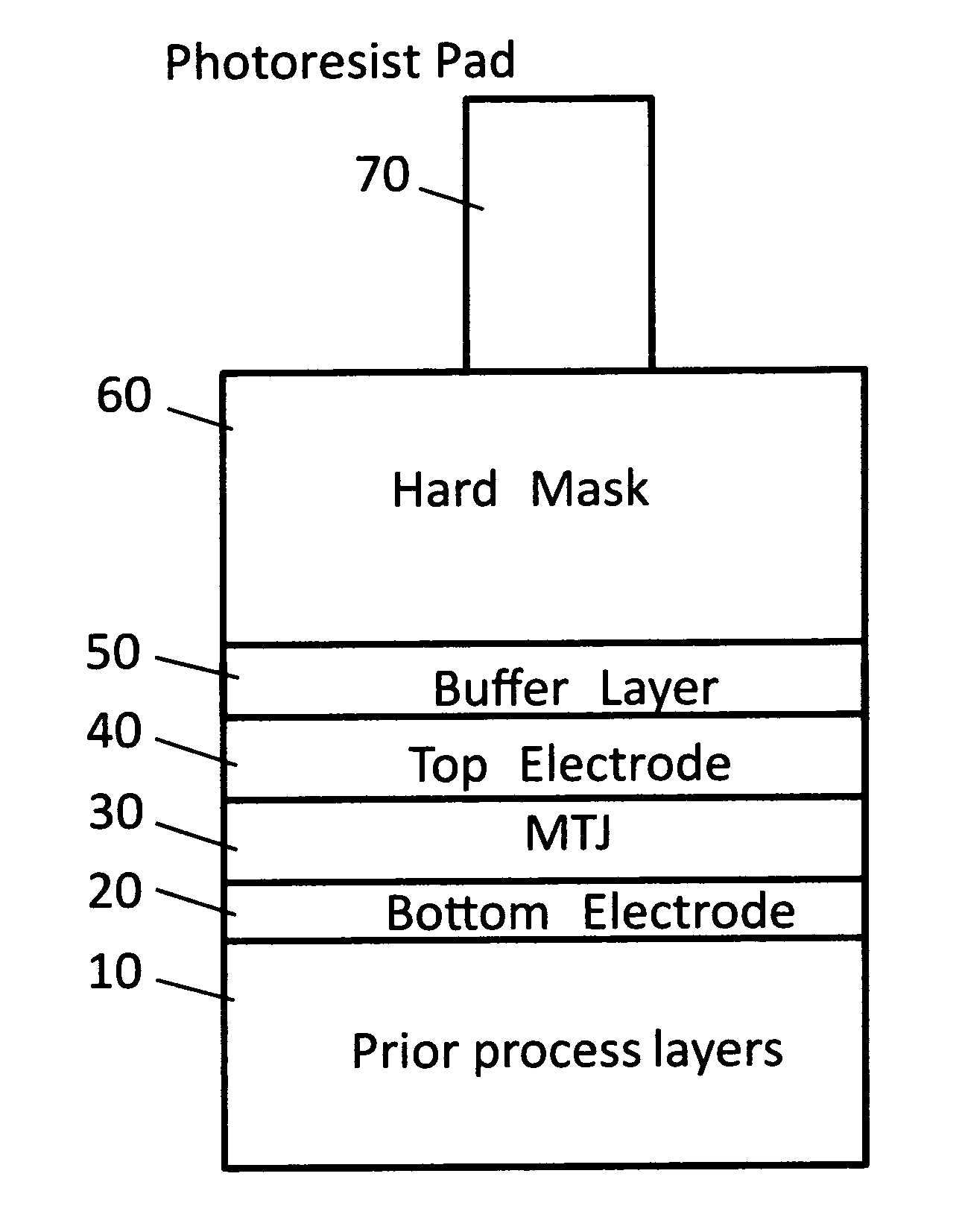
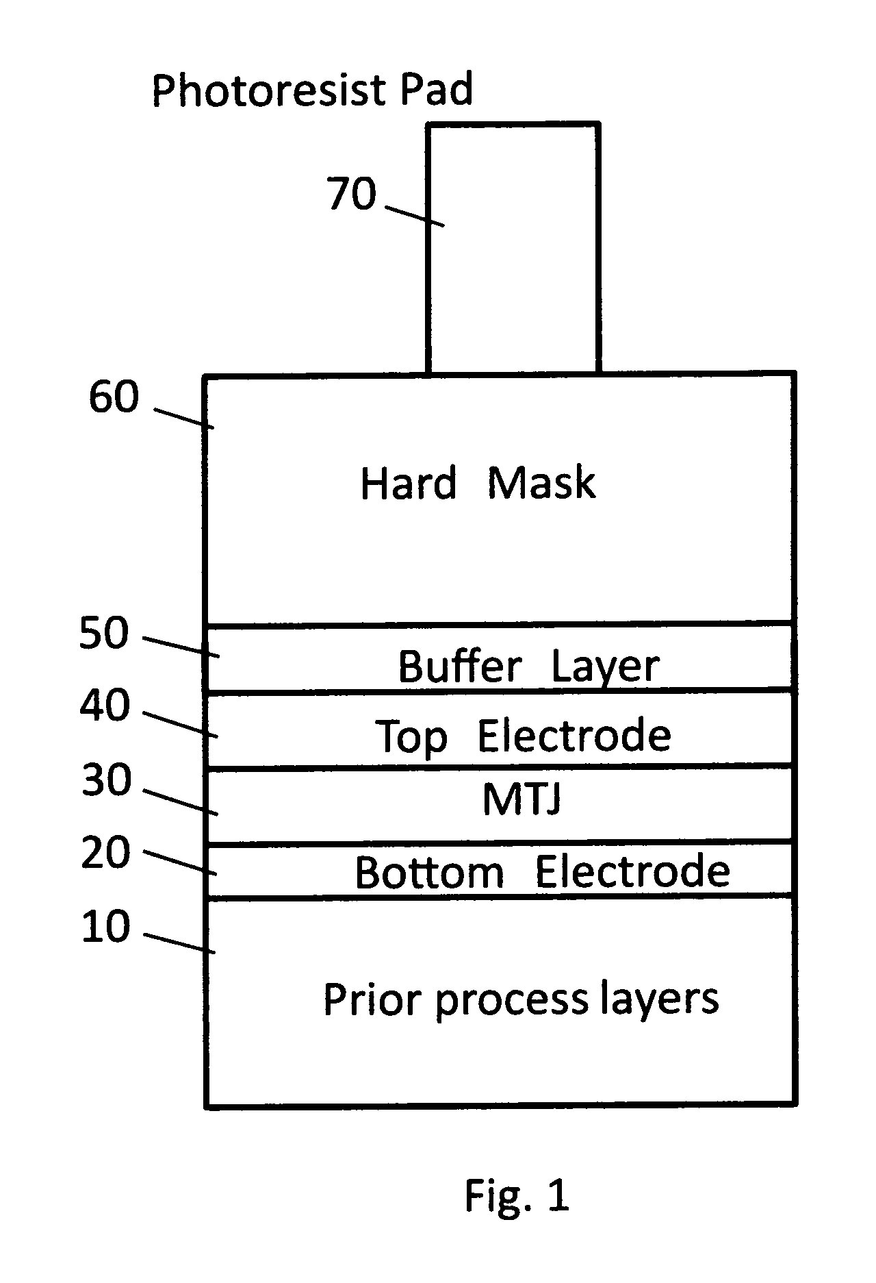
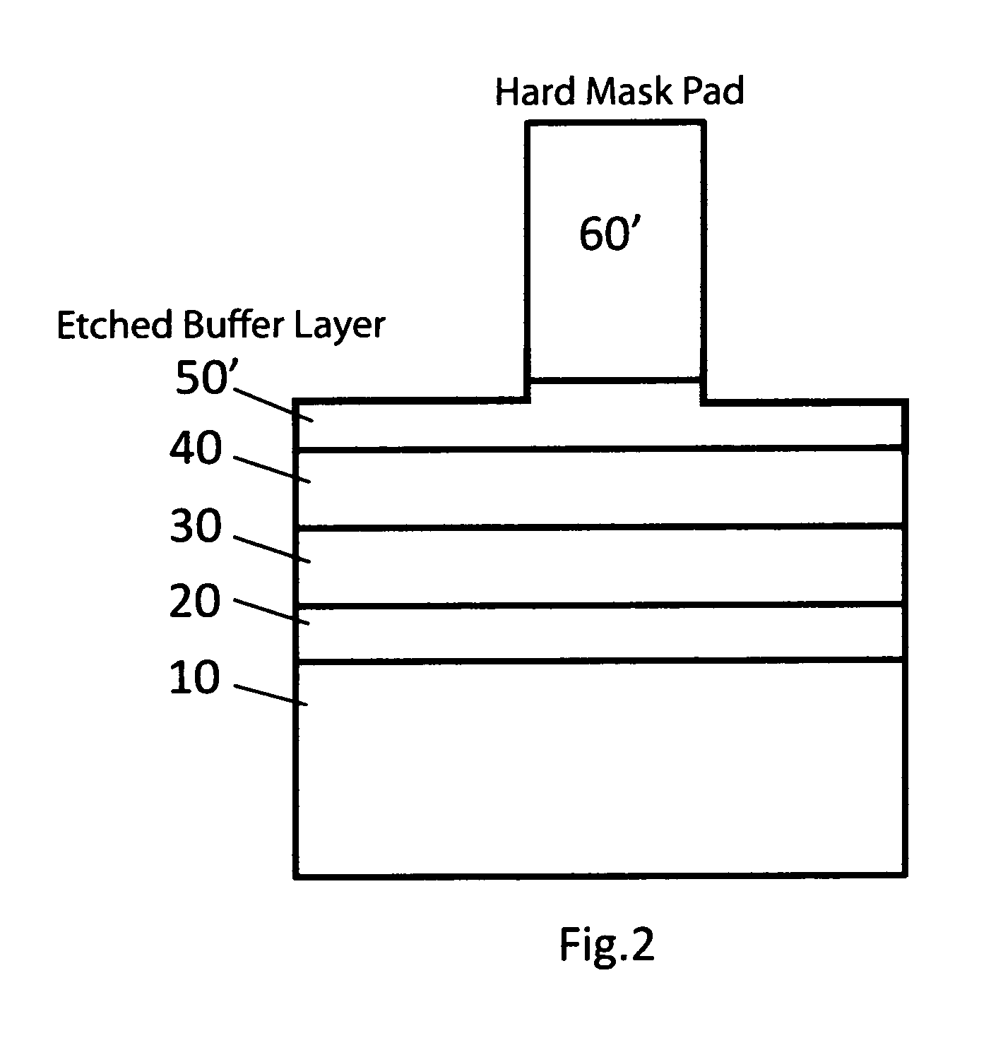
[0025]FIG. 1 and FIG. 2 will be used to describe the first embodiment of the invention. As shown in cross section in FIG. 1, the fabrication process has previously deposited the various thin film layers shown, and a photoresist pad 70 which typically include a bottom antireflective coating (BARC) polymer layer, has been patterned over the selected area. As shown in FIG. 1, a bottom electrode layer 20, an MTJ layer stack 30, a top electrode layer 40, a hard mask buffer layer 50 and a hard mask layer 60 are deposited sequentially. In this embodiment hard mask buffer layer 50 is inserted between a hard mask 60 and top electrode layer 40 to prevent the top electrode surface from being exposed to the etching ambient used to etch the hard mask. To reduce processing steps, the material for buffer layer 50 is selected so that it can be removed by top electrode etching ambient. The preferred materials for the buffer layer 50 are silicon nitride, silicon carbide and their substitutes. A conve...

second embodiment

[0028]FIGS. 3 and 4 illustrate cross sectional views of layers at selected stages of a fabrication process of an MTJ cell according to the second embodiment of the invention. A layer stack structure of the second embodiment is shown in FIG. 3 prior to etching. As in the first embodiment there are two etching processes in this embodiment: a first etch to pattern the hard mask pads and a second etch to pattern the top electrode. Each of these etch processes uses a different etching ambient.

[0029]The bottom electrode layer 20, which is deposited over prior process layers 10, is followed by the MTJ layer stack 30, the top electrode layer 40, a first hard mask layer 60A and a second hard mask layer 61. A conventional hard mask layer material such as silicon oxide, silicon nitride, titanium nitride and their substitutes is selected for the first hard mask layer 60A. The second hard mask layer 61 is preferably a material having a low etching rate in the hard mask and / or top electrode etchi...

third embodiment

[0032]In the third embodiment, the top electrode structure includes two layers: a first top electrode layer 41 of Cu is deposited on the MTJ 30 before the second top electrode layer 40 of a selected metal as shown in FIG. 6. The second top electrode layer 40 can be tantalum (Ta). Using the Ta / Cu embodiment compensates for high etch rate of Cu in MTJ etching ambient. The total top electrode thickness is increased to widen a process window of interconnection process. A photolithography process as described above creates a photoresist pad (not shown) which is followed by etching the second hard mask 61, etching the second top electrode layer 40, etching the first top electrode (Cu) layer 41, etching MTJ 30 and etching half way through the thickness of bottom electrode 20 as shown in FIG. 7. As an option, passivation layer 70 may be deposited to prevent MTJ from oxidation as shown in FIG. 8. From either the stage of FIG. 7 or 8, the standard bottom electrode etching process follows.


PUM


Abstract

Various embodiments of the invention relate to etching processes used in fabrication of MTJ cells in an MRAM device. The various embodiments can be used in combination with each other. The first embodiment adds a hard mask buffer layer between a hard mask and a top electrode. The second embodiment uses a multilayered etching hard mask. The third embodiment uses a multilayered top electrode structure including a first Cu layer under a second layer such as Ta. The fourth embodiment is a two-phase etching process used for the bottom electrode to remove re-deposited material while maintaining a more vertical sidewall etching profile. In the first phase the bottom electrode layer is removed using carbonaceous reactive ion etching until the endpoint. In the second phase an inert gas and/or oxygen plasma is used to remove the polymer that was deposited during the previous etching processes.

Description

FIELD OF THE INVENTION[0001]The disclosure is related to a semiconductor memory and its fabrication process, particularly to a memory element of MRAM (Magnetic Random Access Memory).BACKGROUND OF THE INVENTION[0002]The Back-End-Of-Line (BEOL) memories such as RRAM (Resistive Random Access Memory), PRAM (Phase Change Random Access Memory), MRAM have a resistive memory element that provides high speed access and non-volatility at power off. The memory cell includes a top electrode, a bottom electrode and the resistive memory element in between. The bottom electrode is connected to a control device such as a transistor or a diode. After the layers of the memory device have been patterned, the top electrode is connected to a bit line in a series of process steps collectively referred to as BEOL process which creates metal interconnect wires that are insulated by dielectric material.[0003]A Magnetic Tunnel Junction (MTJ) resistive element for MRAM includes a free layer, a fixed layer and...

Claims


Application Information

Patent Timeline
Patent Type & Authority Applications(United States)
IPC IPC(8): H01L21/8246
CPCH01L29/00H01L43/12H10N50/01
Inventor SATOH, KIMIHIROHUAI, YIMINGZHANG, JINGRANJAN, RAJIV YADAVKESHTBOD, PARVIZMALMHALL, ROGER K.
Owner AVALANCHE TECH
Why Eureka
Try Eureka