Coated semiconductor processing members having chlorine and fluorine plasma erosion resistance and complex oxide coatings therefor

a technology of chlorine and fluorine plasma and semiconductor processing members, which is applied in the direction of metallic material coating process, coating, electric discharge tube, etc., can solve the problems of electrical shorting between two nearby conductors, damage to critical submicron features and functionality of semiconductor devices, and particle generation, so as to improve the tensile bond strength of the coating, reduce the contamination of a working wafer, and reduce the effect of particle generation

Active Publication Date: 2017-10-19
FM INDS
View PDF2 Cites 211 Cited by
  • Summary
  • Abstract
  • Description
  • Claims
  • Application Information

AI Technical Summary

Benefits of technology

[0014]It is also preferred that the semiconductor processing member further comprises a bonding layer between the coating and the body to improve a tensile bond strength of the coating, and that the bond layer is selected from the group consisting of (1) Si and (2) co-phased fully stabilized zirconia and Y2O3.
[0015]According to the present invention, the coating reduces contamination of a working wafer in the semiconductor tool so that an amount of Na measured on the wafer is less than 1×10¹⁴ atom

Problems solved by technology

The etching of material from the chamber walls and various components inside the vacuum chamber results in particle generation, which is undesirable.
These particles can land on the wafers and result in damage to the critical submicron features and functionality of the semiconductor devices that that are being etched or deposited thereon.
Particle generation from the chamber walls in a semiconductor chamber/member can lead to other problems, as well.
The physical presence of eroded metallic particles in parts per million on a process wafer can also cause electrical shorting between two nearby conductors.
In addition, if the generated particles diffuse into the wafer matrix, they can result in uncontrolled ion mobility, the

Method used


Image

  • Coated semiconductor processing members having chlorine and fluorine plasma erosion resistance and complex oxide coatings therefor
  • Coated semiconductor processing members having chlorine and fluorine plasma erosion resistance and complex oxide coatings therefor
  • Coated semiconductor processing members having chlorine and fluorine plasma erosion resistance and complex oxide coatings therefor

Examples


example 1

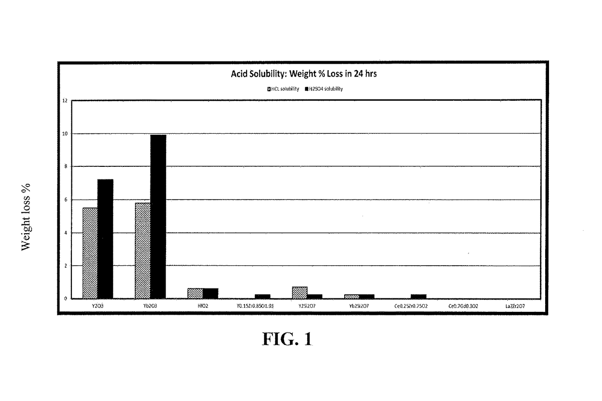
[0047]In view of the undesirable results in Comparative Example 1, powders were then prepared where a solid solution of La2O3 and ZrO2 was made with La2Zr2O7 phase, as verified by X-ray diffraction. Powder samples were prepared using conventional methods of crushing, sieving and spray dry agglomeration to provide an average particle size of 30 μm. The purity of the powder was maintained using powder manufacturing systems lined with plasma sprayed zirconia coatings or polymerics such that all trace elements were less than 50 ppm, all heavy metals were less than 20 ppm, and alkaline metals were less than 10 ppm, as measured by Glow Discharge Mass Spectroscopy (GDMS).

[0048]Coatings were made from this La2Zr2O7 powder using a DC plasma arc system using argon and hydrogen with an envelope of argon around the plasma plume to form La2Zr2O7 coatings. These La2Zr2O7 coatings did not show any weight loss when immersed in HCl for 24 hours. These La2Zr2O7 coatings were then subjected to an ultr...

example 2

[0051]The coating from the coated shell used in Example 1 was stripped off using a grit blast method while preserving the anodization. Then the La2Zr2O7 coating according to Example 1 was reapplied to restore dimensions of the part. The part was again tested in the plasma etch chamber under the same conditions for 5 times with a cleaning cycle in between the process. The part showed no erosion or delamination of the coating from the substrate.

[0052]During the plasma etching processes, Si wafers were also processed, and the contamination levels on the wafers were measured by Mass Spectroscopy using inductively coupled Plasma (MS-ICP). It was found that trace elements on the wafers were less than 10×1010 atoms / cm2. More importantly, heavy metal elements were less than 5×10¹⁰ atoms / cm2, and alkaline metals were less than 2×10¹⁰ atoms / cm2.

[0053]After the above-described testing, the coated part was sectioned and the coating microstructure was revealed, as schematically shown in FIG. 4. ...

example 3

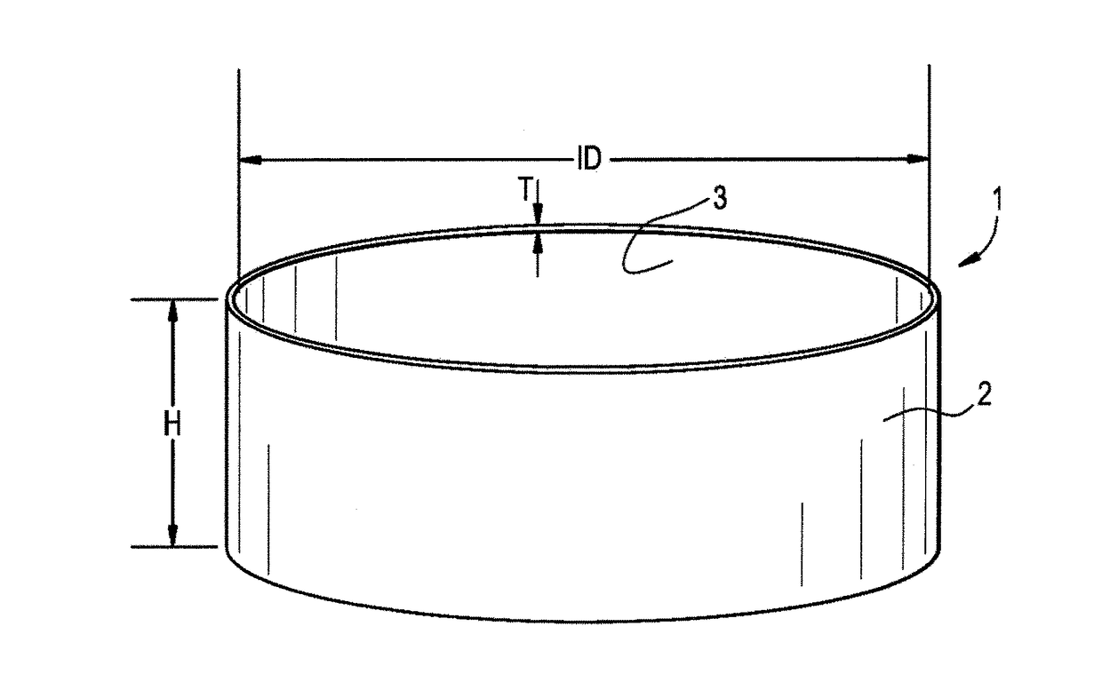
[0055]A part having the shape of a cylindrical shell (14 inch ID and 5 inch height) made of 6061 Al alloy was coated in the same manner as described above in connection with Example 1. This time, the surface of the La2Zr2O7 coating was textured using a series of flexible pads with backing for diamond coated abrasives. Specifically, 60 μm and then 30 μm diamonds were used as abrasives to texture the coated surface to remove only high spots from the coated surface. This flexible finishing method provided the coated surface with a roughness Ra in a range of 80 to 120 pin. The removal of high spots also provided a peak to valley ratio, Rp / Rv of the surface roughness in a range 0.3 to 0.6.

[0056]The part was then cleaned in an ultrasonic bath filled with DI water at 40 KHz at 60° C. for 15 min. Measurement of the particles entrained in the cleaning fluids by a laser particle counter showed a drop of 50% in the total particle count compared to that of Example 1. The part was then dried in ...


PUM

PropertyMeasurementUnit
Fractionaaaaaaaaaa
Fractionaaaaaaaaaa
Fractionaaaaaaaaaa

Abstract

A semiconductor processing member is provided, including a body and a plasma spray coating provided on the body. The coating is an ABO or ABCO complex oxide solid solution composition, where A, B and C are selected from the group consisting of La, Zr, Ce, Gd, Y, Yb and Si, and O is an oxide. The coating imparts both chlorine and fluorine plasma erosion resistance, reduces particle generation during plasma etching, and prevents spalling of the coating during wet cleaning of the semiconductor processing member.

Description

FIELD OF THE INVENTION[0001]This invention relates to semiconductor processing chambers or members operating with plasma assisted etching or deposition processes. More specifically, the invention relates to complex oxide coatings applied on vacuum and plasma chamber components to prevent particle generation, to provide dielectric protection, to provide wet clean resistance, to maintain a high purity environment for the creation of critical dimensions and features of semiconductor devices produced therein and to provide an extended life for the coated chamber components.BACKGROUND OF THE INVENTION[0002]Processing chambers used for making semiconductor devices involve deposition and etching processes performed in vacuum environments. These processes also require plasma chemistries to etch or deposit conductors and dielectric materials on various substrates (wafers). These wafers are mostly made of Si, but may also be made of GaAs or GaN. During such plasma processes, where plasma gene...

Claims


Application Information

Patent Timeline
IPC IPC(8): H01J37/32C23C4/134C23C4/11C23C4/02
CPCH01J37/32495C23C4/134H01J2237/334C23C4/02H01J2237/332C23C4/11C23C16/4404
Inventor NAIM, MAHMOODHAMMERICH, DAVID
Owner FM INDS
Why Eureka
Try Eureka