Methods And Systems For Overlay Measurement Based On Soft X-Ray Scatterometry

a scatterometry and soft x-ray technology, applied in the field of metalrology systems and methods, can solve the problems of difficult optical radiation penetration to the bottom layer, difficult characterization, and increased difficulty in characterization, so as to achieve enhanced sensitivity to overlay among the layers corresponding with the predetermined subset of scattering vectors, and sufficient periodicity.

Active Publication Date: 2021-07-08
KLA TENCOR TECH CORP
View PDF0 Cites 5 Cited by
  • Summary
  • Abstract
  • Description
  • Claims
  • Application Information

AI Technical Summary

Benefits of technology

[0030]In another aspect, the actual device target is aperiodic. By calibrating overlay measurements to a reference measurement, SXR scatterometry techniques can be applied to estimate overlay of aperiodic structures based on measurements of design rule targets with sufficient periodicity. This effectively overcomes the limitation of scatterometric measurements requiring the measured target to be periodic or approximately periodic.
[0031]In some embodiments, a multiple layer overlay metrology target is designed with different pitch at different layers such that a diffraction order arising from one layer constructively interferes with a different diffraction order of another layer. Conversely, intensity measurements detected at different order number pairs not subject to constructive interference in overlay are dominated by shape parameters. Thus, in some embodiments, a metrology overlay target is designed with specific grating structures to increase sensitivity to overlay at specific grating order pairs, and also provide intensity data useful for estimation of shape parameter values.
[0032]In some embodiments, a multiple layer overlay metrology target is designed with different pitch orientations at different layers such that a diffraction order arising from one layer constructively interferes with a different diffraction order of another layer. In general, a set of layers having different periodicities (e.g., different grating pitches), different pitch orientations, or any combination thereof, gives rise to a set of scattering vectors, each associated with a different layer. The overlay metrology target is designed such that a predetermined subset of the scattering vectors are aligned. In this manner, the sensitivity to overlay among the layers corresponding with the predetermined subset of scattering vectors is enhanced.

Problems solved by technology

As devices (e.g., logic and memory devices) move toward smaller nanometer-scale dimensions, characterization becomes more difficult.
Devices incorporating complex three-dimensional geometry and materials with diverse physical properties contribute to characterization difficulty.
For example, modern memory structures are often high-aspect ratio, three-dimensional structures that make it difficult for optical radiation to penetrate to the bottom layers.
Optical metrology tools utilizing infrared to visible light can penetrate many layers of translucent materials, but longer wavelengths that provide good depth of penetration do not provide sufficient sensitivity to small anomalies.
Similarly, electron based metrology tools suffer from inadequate depth of penetration without damaging the sample.
As a result, the parameters characterizing the target often cannot be reliably decoupled with available measurements.
For some structural parameters, such as edge placement error (EPE), there is currently no high throughput (e.g., optical) measurement solution.
However, these approaches have not reliably overcome fundamental challenges associated with measurement of many advanced targets (e.g., complex 3D structures, structures smaller than 10 nm, structures employing opaque materials) and measurement applications (e.g., line edge roughness and line width roughness measurements).
Unfortunately, these specialized target structures often do not conform to the design rules of the particular semiconductor manufacturing process being employed to generate the electronic device.
This leads to errors in estimation of overlay errors associated with actual device structures that are manufactured in accordance with the applicable design rules.
In one example, image-based optical overlay metrology is severely limited by the resolution of imaging at optical wavelengths.
Moreover, the accuracy of this measurement approach degrades dramatically in the presence of any asymmetry in any of the layers where overlay is measured.
In addition, this approach cannot differentiate between positive and negative overlay errors in a single measurement.
In addition, the accuracy of this approach degrades dramatically in the presence of any asymmetry in any of the layers where overlay is measured.
Decreasing the optical wavelength of the illumination into the deep ultraviolet and vacuum ultraviolet range does not help as these photons are attenuated and do not sufficiently penetrate multiple layer structures to reach underlying patterns required to evaluate overlay and edge placement error.
However, electron based metrology systems are destructive when employed to measure actual devices.
In addition, electron based metrology systems are low throughput.
In addition, electron based metrology systems are top-down imaging systems that provide very limited three dimensional measurement capability.
For example, when SEM is employed to measure overlay between overlapping gratings, it loses the ability to measure CD and EPE due to increased point spread function with penetration depth.
In general, SEM achieves intermediate resolution levels, but is unable to penetrate structures to sufficient depth without destroying the sample.
In addition, the required charging of the specimen has an adverse effect on imaging performance.
Atomic force microscopes (AFM) and scanning-tunneling microscopes (STM) are able to achieve atomic resolution, but they can only probe the surface of the specimen.
In addition, AFM and STM microscopes require long scanning times.
Transmission electron microscopes (TEM) achieve high resolution levels and are able to probe arbitrary depths, but TEM requires destructive sectioning of the specimen.
Unfortunately, the absolute registration measurement technique requires an accurate stage, adds complexity to the measurement tool, and limits throughput.
Furthermore, the technique may not perform well on pattern-over-pattern targets or device structures.
Currently there is no high-throughput, optical metrology solution for EPE measurements and many design-rule overlay measurement applications.
In addition, the absence of adequate metrology makes it challenging to define control schemes to improve device yield.
Future metrology applications present challenges for metrology due to increasingly small resolution requirements, multi-parameter correlation, increasingly complex geometric structures, and increasing use of opaque materials.
Furthermore, the overlay error associated with the measurement target is determined based on modulations in the plurality of intensities within each of the one or more nonzero diffraction orders at each of the multiple measurement instances.
In some embodiments, a multiple layer overlay metrology target is designed with different pitch orientations at different layers such that a diffraction order arising from one layer constructively interferes with a different diffraction order of another layer.

Method used


Image

  • Methods And Systems For Overlay Measurement Based On Soft X-Ray Scatterometry
  • Methods And Systems For Overlay Measurement Based On Soft X-Ray Scatterometry
  • Methods And Systems For Overlay Measurement Based On Soft X-Ray Scatterometry

Examples


Embodiment Construction

[0046]Reference will now be made in detail to background examples and some embodiments of the invention, examples of which are illustrated in the accompanying drawings.

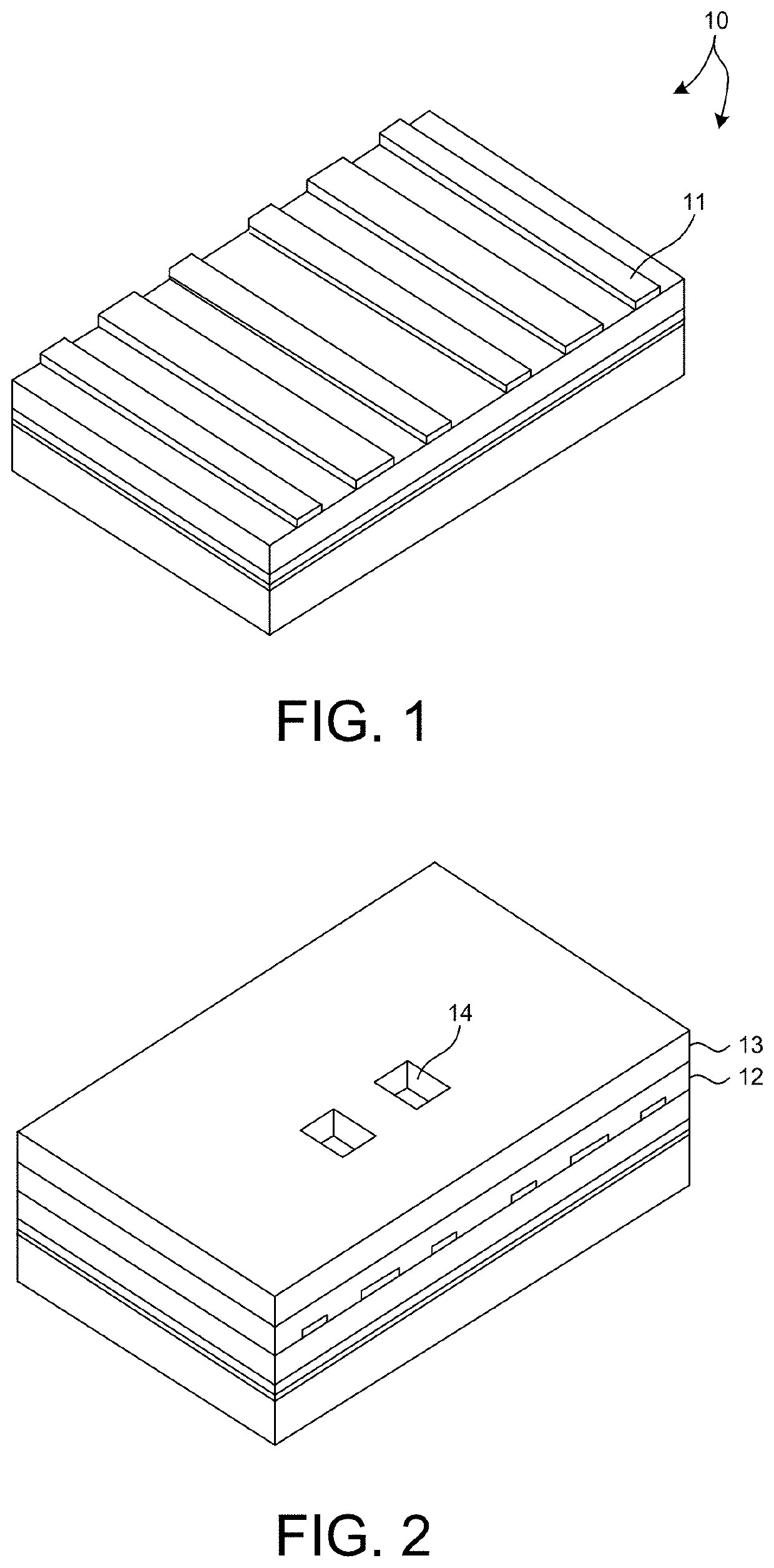
[0047]FIG. 1 depicts a hardmask pattern of line structures 11 fabricated in a static random access memory (SRAM) area 10 of a microelectronic chip. The complex layout of the active region is created by combining multiple patterning techniques with cut masks. Cut masks selectively remove portions of the hardmask layer that is used to pattern the substrate into active regions. FIG. 2 depicts a bottom anti-reflective coating (BARC) layer 12 and a resist layer 13 disposed on top of the pattern of line structures depicted in FIG. 1. The resist layer is used to selectively remove part of the hardmask pattern below the openings 14 of the resist layer 13. As depicted in FIG. 1, the hardmask pattern of line structures 11 is buried by the BARC layer 12, even within the openings 14 of the resist layer 13.

[0048]To provide adequat...


PUM

PropertyMeasurementUnit
energyaaaaaaaaaa
energyaaaaaaaaaa
roughnessaaaaaaaaaa

Abstract

Methods and systems for performing overlay and edge placement errors based on Soft X-Ray (SXR) scatterometry measurement data are presented herein. Short wavelength SXR radiation focused over a small illumination spot size enables measurement of design rule targets or in-die active device structures. In some embodiments, SXR scatterometry measurements are performed with SXR radiation having energy in a range from 10 to 5,000 electronvolts. As a result, measurements at SXR wavelengths permit target design at process design rules that closely represents actual device overlay. In some embodiments, SXR scatterometry measurements of overlay and shape parameters are performed simultaneously from the same metrology target to enable accurate measurement of Edge Placement Errors. In another aspect, overlay of aperiodic device structures is estimated based on SXR measurements of design rule targets by calibrating the SXR measurements to reference measurements of the actual device target.

Description

CROSS REFERENCE TO RELATED APPLICATION[0001]The present application for patent claims priority under 35 U.S.C. § 119 from U.S. provisional patent application Ser. No. 62 / 958,089, entitled “System and Method for Measuring Overlay and Edge Placement Error With Soft X-ray Scatterometry,” filed Jan. 7, 2020, the subject matter of which is incorporated herein by reference in its entirety.TECHNICAL FIELD[0002]The described embodiments relate to metrology systems and methods, and more particularly to methods and systems for improved measurement accuracy.BACKGROUND INFORMATION[0003]Semiconductor devices such as logic and memory devices are typically fabricated by a sequence of processing steps applied to a specimen. The various features and multiple structural levels of the semiconductor devices are formed by these processing steps. For example, lithography among others is one semiconductor fabrication process that involves generating a pattern on a semiconductor wafer. Additional examples ...

Claims


Application Information

Patent Timeline
Patent Type & Authority Applications(United States)
IPC IPC(8): G01B15/00G03F7/20
CPCG01B15/00G03F7/70633H01L27/1104G01B2210/56G03F7/70516H01L22/12H01L22/20G01B15/02H01L21/0276H10B10/12
Inventor SHCHEGROV, ANDREI V.GUTMAN, NADAVKUZNETSOV, ALEXANDERGELLINEAU, ANTONIO ARION
Owner KLA TENCOR TECH CORP
Why Eureka
Try Eureka