Single-mode micro-laser based on single whispering gallery mode optical microcavity and preparation method thereof
a single-mode, optical microcavity technology, applied in the direction of lasers, laser optical resonator construction, semiconductor lasers, etc., can solve the problems of increasing the bending radiation loss of the microcavity, significantly increasing the pump threshold and laser linewidth of the micro-laser, and reducing the quality factor of the microcavity. , to achieve the effect of narrow line width, selective reduction of the quality factor of the fundamental spatial mode of the optical microcav
- Summary
- Abstract
- Description
- Claims
- Application Information
AI Technical Summary
Benefits of technology
Problems solved by technology
Method used
Image
Examples
embodiment 1
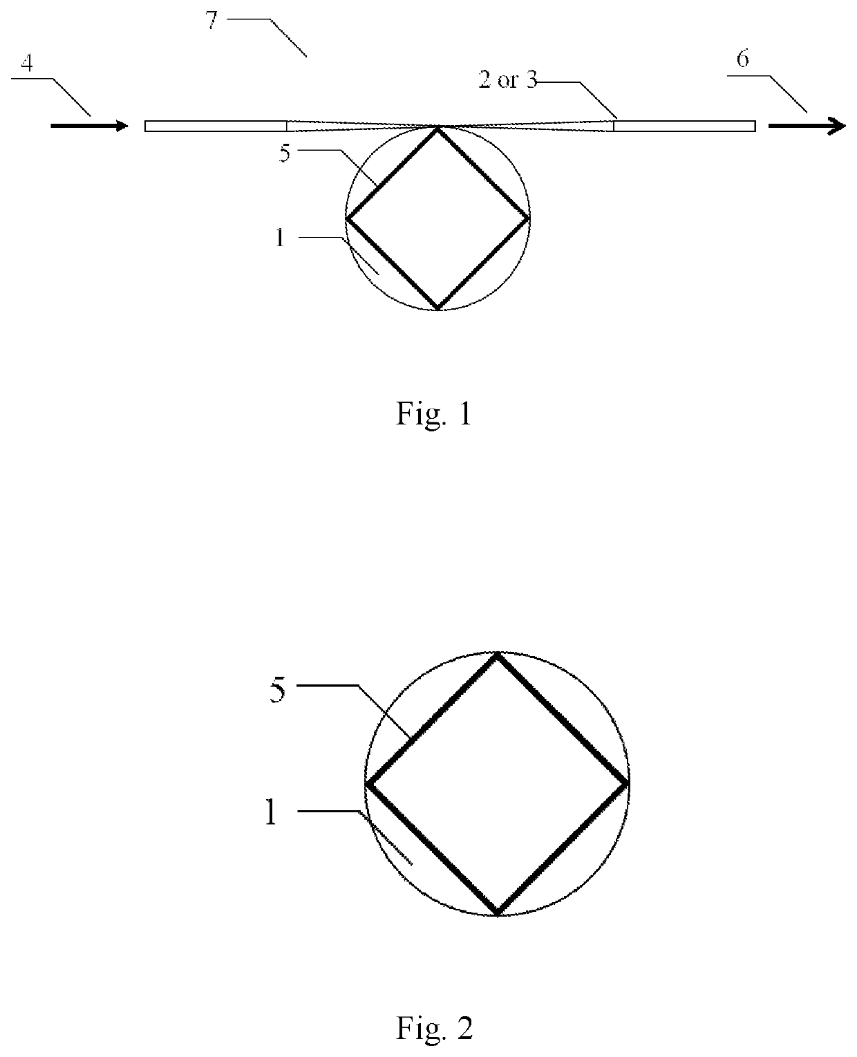
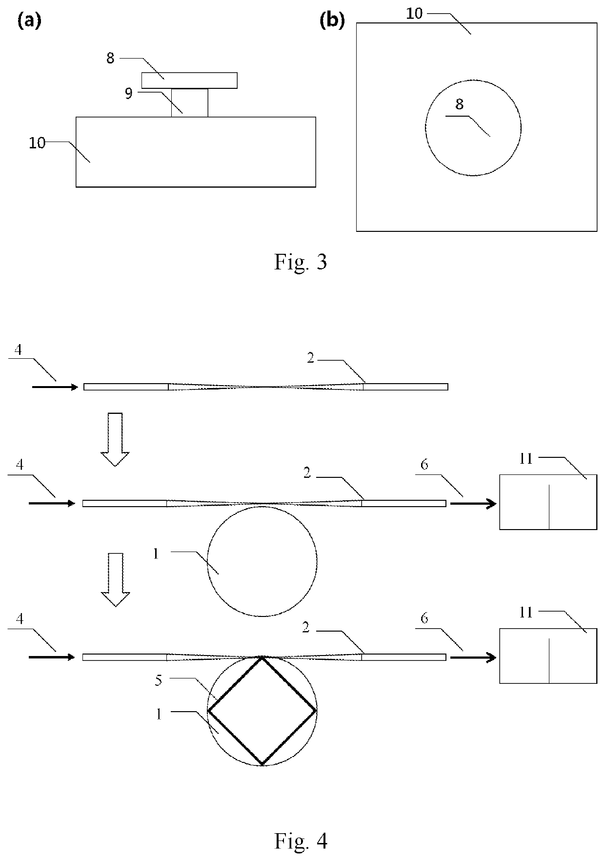
[0034]1) Coupling an optical fiber cone to a lithium niobate film optical microcavity doped with erbium ions, wherein referring to FIG. 4, a wafer of a lithium niobate film 8 doped with 1 mol % erbium ions is illustrated; plating a 700 nm-thick chromium film as a mask, and etching the optical microcavity of a required size by a femtosecond laser; wherein the optical microcavity has a diameter of about 30 microns, and is located on a 2 μm-thick silicon dioxide layer pillar 9 supported by a underlying lithium niobate substrate 10; a free spectral range of the optical microcavity near a wavelength of 1550 nm is about 13 nm, which is about half of an erbium ion gain bandwidth (1535˜1560 nm); processing the optical microcavity etched by the femtosecond laser with a chemical mechanical polishing technology (R. Wu, et al., Opt. Lett., Vol. 43, P 4116-4118, 2018) to obtain a whispering gallery mode optical microcavity 1 which has a smooth edge and is doped with the erbium ions, then perform...
embodiment 2
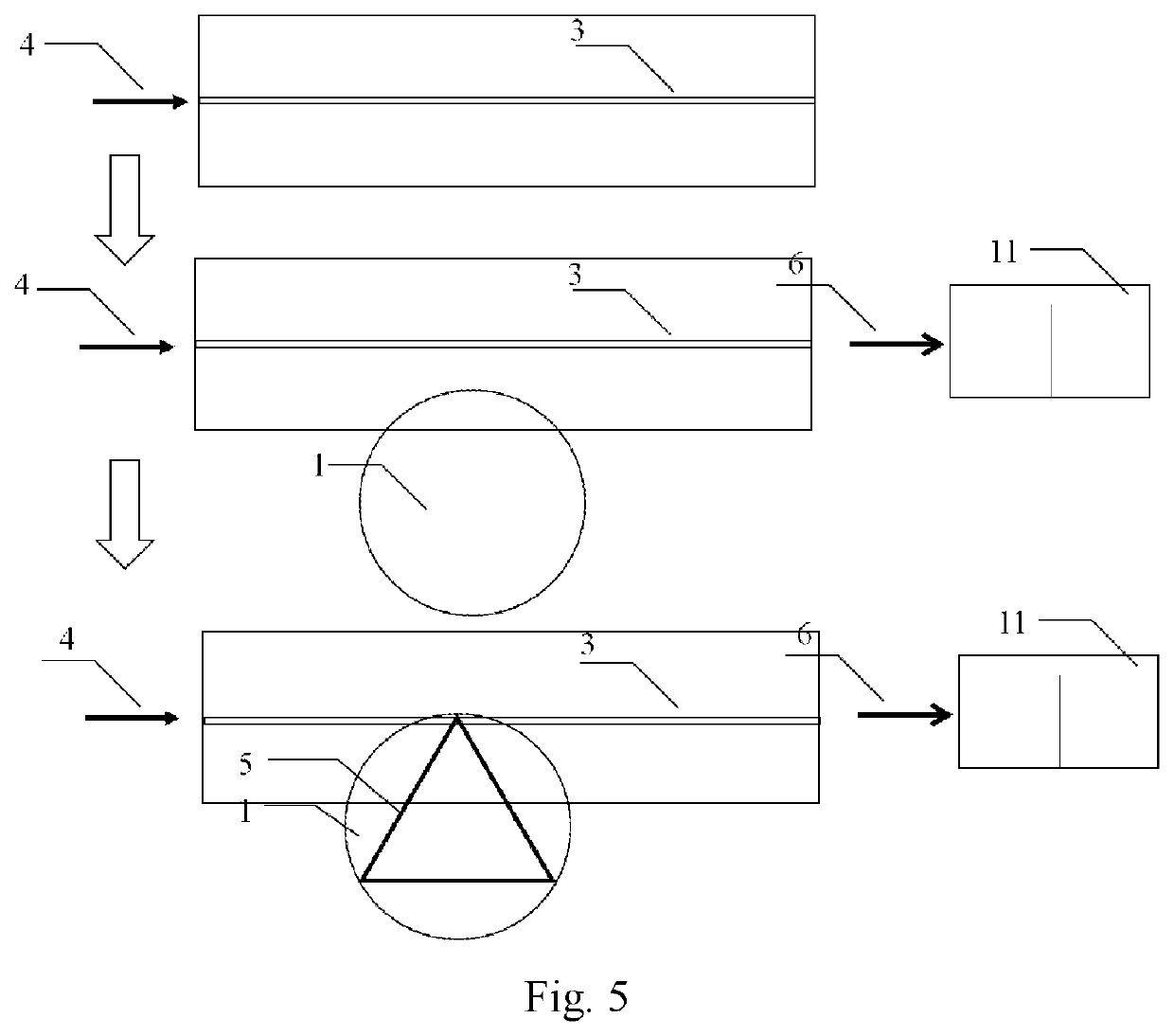
[0041]Referring to FIG. 5, coupling of an optical waveguide and an optical microcavity containing quantum dots is illustrated.
[0042]1) Etching the optical microcavity containing the quantum dots of a required size by a femtosecond laser; wherein after etching a free spectral range of the optical microcavity is at least ½ of a spectral width of a material containing the quantum dots; processing the optical microcavity with a chemical mechanical polishing technology (R. Wu, et al., Opt. Lett., Vol. 43, P 4116-4118, 2018) to obtain an optical microcavity with a smooth edge, wherein before polishing, a golden velvet polishing pad is used for carefully cleaning, so as to prevent small particles from scratching the optical microcavity, and an ultrasonic method can be used for deep cleaning; cleaning the polished optical microcavity by ultrasonic and cotton swab scrubbing methods to remove organic matters and particles on the surface, making a surface of the optical microcavity cleaner and...
PUM
| Property | Measurement | Unit |
|---|---|---|
| diameter | aaaaa | aaaaa |
| diameter | aaaaa | aaaaa |
| spectral width | aaaaa | aaaaa |
Abstract
Description
Claims
Application Information


