Silicon wafer and epitaxial silicon wafer utilizing same

a technology of epitaxial silicon and silicon wafer, which is applied in the direction of after-treatment details, transportation and packaging, and compounds of silicon, etc., can solve the problems of affecting reducing the performance characteristics of devices, and producing problems

Inactive Publication Date: 2003-05-27
SUMITOMO MITSUBISHI SILICON CORP
View PDF7 Cites 20 Cited by
  • Summary
  • Abstract
  • Description
  • Claims
  • Application Information

AI Technical Summary

Problems solved by technology

Thus, problems are produced not only by such defects as oxygen-induced stacking faults (hereinafter referred to as "OSFs"), which manifest themselves in device manufacturing processes and lower the performance characteristics of the devices, but also by micro defects, namely grown-in defects, which are formed in the step of crystal growth and greatly affect the performance characteristics of the devices.
When formed and grown on the wafer surface, which constitutes active regions of devices, they cause a leakage current and deteriorate the device characteristics.
Dislocation clusters, another kind of grown-in defects, too, give no good devices when these are formed thereon.
For attaining such a defect-free state, however, the condition ranges are restricted and it is not easy to stably realize the increase in pulling rate and the enlargement in single crystal diameter, for instance, on the place of mass production.
Recent trends toward decreases in temperature in device production steps and toward reductions in high temperature heat treatment time have rendered the effects of OSFs less injurious and made them less meaningful as factors deteriorating device characteristics.
On the other hand, as the trend toward miniaturization of circuits increases, laser scattering tomography defects, which are grown-in defects, have become causative of decreases in the yield of conforming products and it is now an important problem to reduce the density of laser scattering tomography defects.
While, in the oxygen precipitation promoted region, oxide precipitates forming BMDs can be obtained, the formation of BMDs in the oxygen precipitation inhibited region tends to be difficult.
However, because of the high density occurrence of laser scattering tomography defects small in size, it has been scarcely possible to obtain wafers satisfactory in time zero dielectric breakdown characteristic.
The wafer at the position E is excellent from the viewpoint on the defect-freeness but the drawback thereof is that a sufficiently large number of BMDs cannot be formed.
There is the problem, however, that when they are used as substrates for epitaxial wafers, many traces of defects remain upon epitaxial layer formation, hence satisfactory layers are not always obtained.
It seemed, however, that there be a region where defects are small in size and low in density between the region of occurrence of laser scattering tomography defects and the denuded zone.
It is not always easy to increase the temperature gradient in the pulling axis direction and control that temperature gradient in a manner such that the central portion of the single crystal shows a greater gradient than the peripheral surface portion.

Method used


Image

  • Silicon wafer and epitaxial silicon wafer utilizing same
  • Silicon wafer and epitaxial silicon wafer utilizing same
  • Silicon wafer and epitaxial silicon wafer utilizing same

Examples


example 1

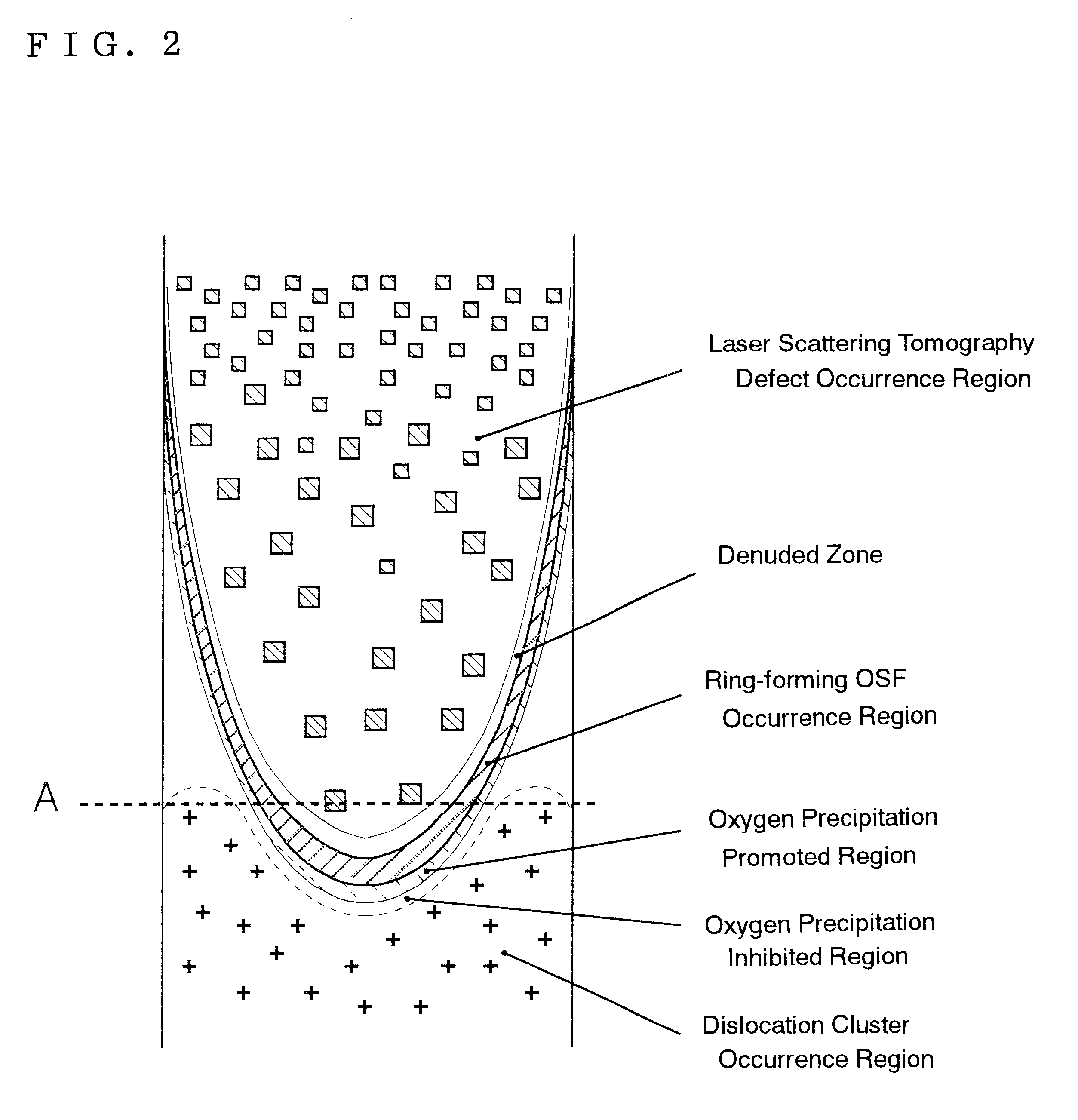
Using an apparatus whose sectional structure was as schematically shown in FIG. 5, experiments were made to grow single crystals with an intended diameter of 210 mm and a body length of 1,000 mm. In this figure, the heat shield 7 had a structure such that the outer shell was made of graphite and the inside was filled with graphite felt. The outer diameter of the portion inserted in the crucible was 480 mm, the smallest diameter S at the lower end was 270 mm, the width W in the radial direction was 105 mm, and the inner surface had the shape of an inverse truncated cone beginning with the lower end, with an inclination of 21.degree. against the vertical direction. The crucible 1 used had an inside diameter of 550 mm, the height H of the heat shield 7 from the melt surface at the lower end was 60 mm.

The crucible was charged with 120 kg of high purity polycrystalline silicon, and the p-type dopant boron was added so that the single crystal might have an electric resistance of about 10 ...

example 2

Using the same wafer X as described above in Example 1, a wafer with oxide precipitates formed therein was prepared by 2 hours of heating at 780.degree. C. in a nitrogen gas atmosphere containing 30% of oxygen, followed by 8 hours of heat treatment at 1,000.degree. C. The cleavage surface of this wafer was observed and oxide precipitates, which are BMDs, were observed at a density of 1.1.times.10.sup.5 / cm.sup.2. This wafer was examined for surface grown-in defects, time-zero dielectric breakdown, gettering capability and, further, characteristics of devices formed and conforming product percentage and so forth. As a result, it was confirmed that it was superior to the conventional wafers.

example 3

The same wafer X according to the invention as shown in Example 1 and the same prior art wafer C for comparison were used and subjected to 1 hour of heating treatment at 1,200.degree. C. in a high-purity hydrogen gas atmosphere at a temperature increasing or decreasing rate of 3.degree. C. / min. After subjecting the treated wafers to SC-1 washing (washing with a mixed solution composed of aqueous ammonia, aqueous solution of hydrogen peroxide and ultrapure water=1:1:15), they were measured for the density of defects having a size not smaller than 0.8 .mu.m using a surface testing apparatus (KLA-Tencor model SP-1). After surface observation, the 1-.mu.m-thick wafer surface layer was polished off using a mirror polishing machine and, after SC-1 washing, the new surface was examined for the defects mentioned above. This procedure was repeated and the thickness of the denuded layer formed on the surface was measured.

As a result, the wafer C was found to have a 2- to 3-.mu.m-thick denuded...


PUM

PropertyMeasurementUnit
mean sizeaaaaaaaaaa
sizeaaaaaaaaaa
melting pointaaaaaaaaaa

Abstract

A silicon wafer characterized in that the laser scattering tomography defect occurrence region accounts for at least 80% of the wafer surface area and that the laser scattering tomography defects have a mean size of not more than 0.1 mum, with the density of those defects which exceed 0.1 mum in size being not more than 1x105 cm-3, and wafers derived from this wafer as the raw material by heat treatment for oxide precipitate formation, by heat treatment for denuded layer formation or by epitaxial layer formation on the surface are useful as semiconductor materials.

Description

The present invention relates to a silicon wafer to be used as a semiconductor material and having a very low surface defect density with bulk micro defects (BMDs) uniformly and sufficiently abundantly formed therein, and to an epitaxial silicon wafer derived from the silicon wafer by forming an epitaxial layer thereon.DESCRIPTION OF THE PRIOR ARTSemiconductor silicon wafers are sliced from silicon single crystals and the method most widely employed for the production of such silicon single crystals is the Czochralski method (CZ method) of pulling single crystals.The CZ method comprises dipping a seed crystal in a molten silicon placed in a quartz crucible and pulling up the seed crystal to thereby allow a single crystal to grow. With the advancement in the technology of pulling silicon single crystals, it has now become possible to produce less defective, dislocation-free, large single crystals. Semiconductor devices are produced from wafers or substrates prepared from single cryst...

Claims


Application Information

Patent Timeline
Patent Type & Authority Patents(United States)
IPC IPC(8): C30B15/14C30B15/00C30B29/06C30B33/02H01L21/208H01L21/322H01L21/324
CPCC30B15/14C30B15/203C30B29/06C30B15/206Y10T428/21C30B15/00
Inventor MURAKAMI, HIROKIEGASHIRA, KAZUYUKI
Owner SUMITOMO MITSUBISHI SILICON CORP
Why Eureka
Try Eureka