Semiconductor device and method for forming the same

a semiconductor and gate technology, applied in the direction of semiconductor devices, electrical devices, transistors, etc., can solve the problems of low reproducibility, unobtainable excellent characteristics, and unobtainable excellent characteristics with high reproducibility, and achieve the effect of improving the flatness of the devi

Inactive Publication Date: 2003-09-23
SEMICON ENERGY LAB CO LTD
View PDF162 Cites 80 Cited by
  • Summary
  • Abstract
  • Description
  • Claims
  • Application Information

AI Technical Summary

Benefits of technology

An object of this invention is to provide an insulating gate type of semiconductor device (an insulated gate field effect transistor) and a producing method there

Problems solved by technology

However, this excellent characteristic has been unobtainable with high reproducibility.
However, this excellent characteristic has been also unobtainable with high reproducibility.
One cause of the low reproducibility resides in the invasion (contamination) of movable ions such as natrium, etc. from the external.
Particularly in the sputtering method, the risk of the invasion (contamination) of natrium ions is large.
However, it is difficult to form the phosphosilicate glass at a low temperature which is aimed by the inventions as disclosed in the above Patent Applications.
In addition, if the formation of the phosphosilicate glass at such a low temperature is attempted, for example by injecting phosphorus into a silicon oxide gate insulating film using an ion doping method, there frequently occurs a problem that a large number of defects occur in the gate insulating film and thus the characteristic of the TFT is rather deteriorated.
In addition, high voltage of 100 to 300 V is required for the anodic oxidation, and thus there is a risk that the gate insulating film is damaged by the high voltage.
Accordingly, there occurs a case where the gate electrode is damaged by this current.
However, it is difficult to form a contact hole in the aluminum oxide.
Therefore, an element structure having high unevenness (a large number of recesses and projections) causes ununiformity of electric field, so that not only the characteristic of the element is deteriorated, but also the element itself suffers a mechanical damage.
As described above, the planar type of TFT having the structure as shown in FIG. 12 is characterized in that unevenness of the structure is low, however, has several problems.
The maximum significant problem resides in that a hole is formed in an electrode, and thus unevenness becomes higher at the contact hole portion, so that disconnection or contact failure occurs at the portion.
Particularly, an unit part of a large-area circuit in which a TFT is used, ha

Method used


Image

  • Semiconductor device and method for forming the same
  • Semiconductor device and method for forming the same
  • Semiconductor device and method for forming the same

Examples


embodiment 1

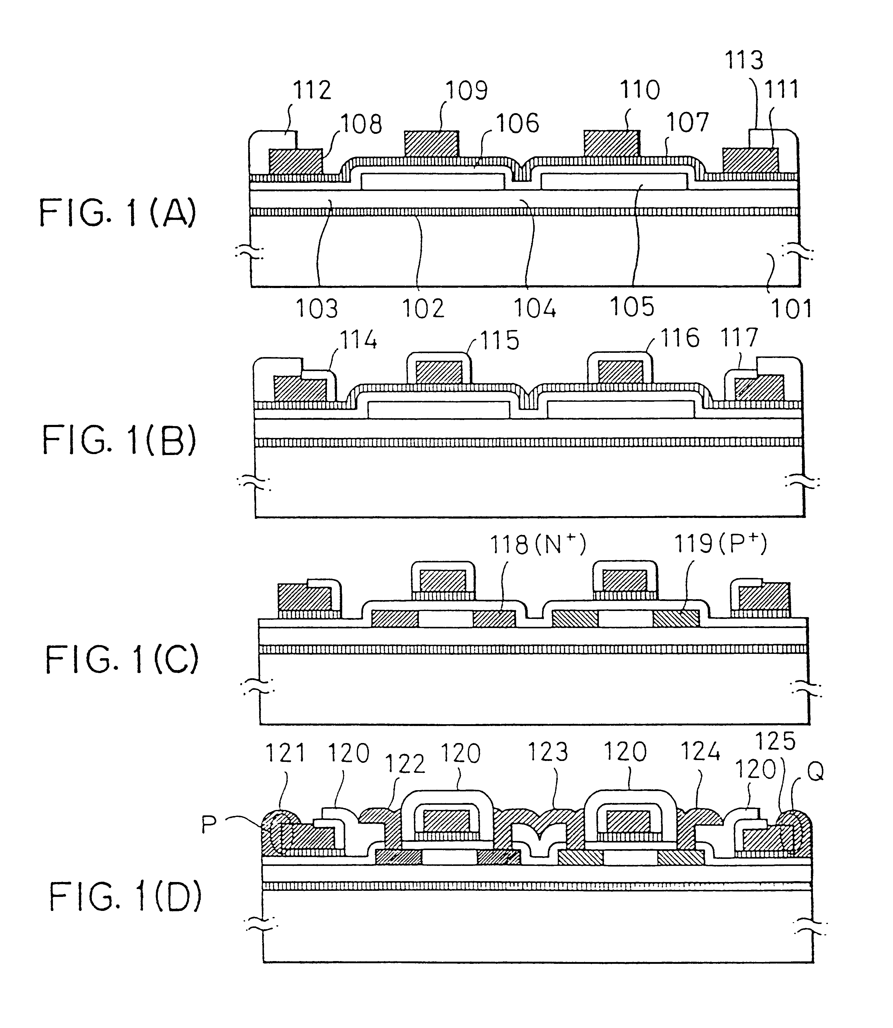
FIG. 1 is cross-sectional views showing a manufacturing process of an embodiment. The detailed conditions of this embodiment are substantially identical to those of Japanese Patent Application No. 3-237100 which was filed by the inventor of this application, et.al, and the description thereof is not particularly made.

An N--O glass produced by Nippon Electric Glass Co., Ltd. was used as a substrate 101. This glass has high strain temperature, but contains a large amount of lithium and natrium. Therefore, in order to prevent invasion of these movable ions from the substrate, a silicon nitride film 102 was formed in thickness of 10 to 50 nm on the substrate by a plasma CVD method or a low pressure CVD method. Further, a silicon oxide film serving as a sealer was formed in thickness of 100 to 800 nm by a sputtering method. An amorphous silicon film was formed on the silicon oxide film in thickness of 20 to 100 nm by the plasma CVD method, and annealed at 600.degree. C. for 12 to 72 hour...

embodiment 2

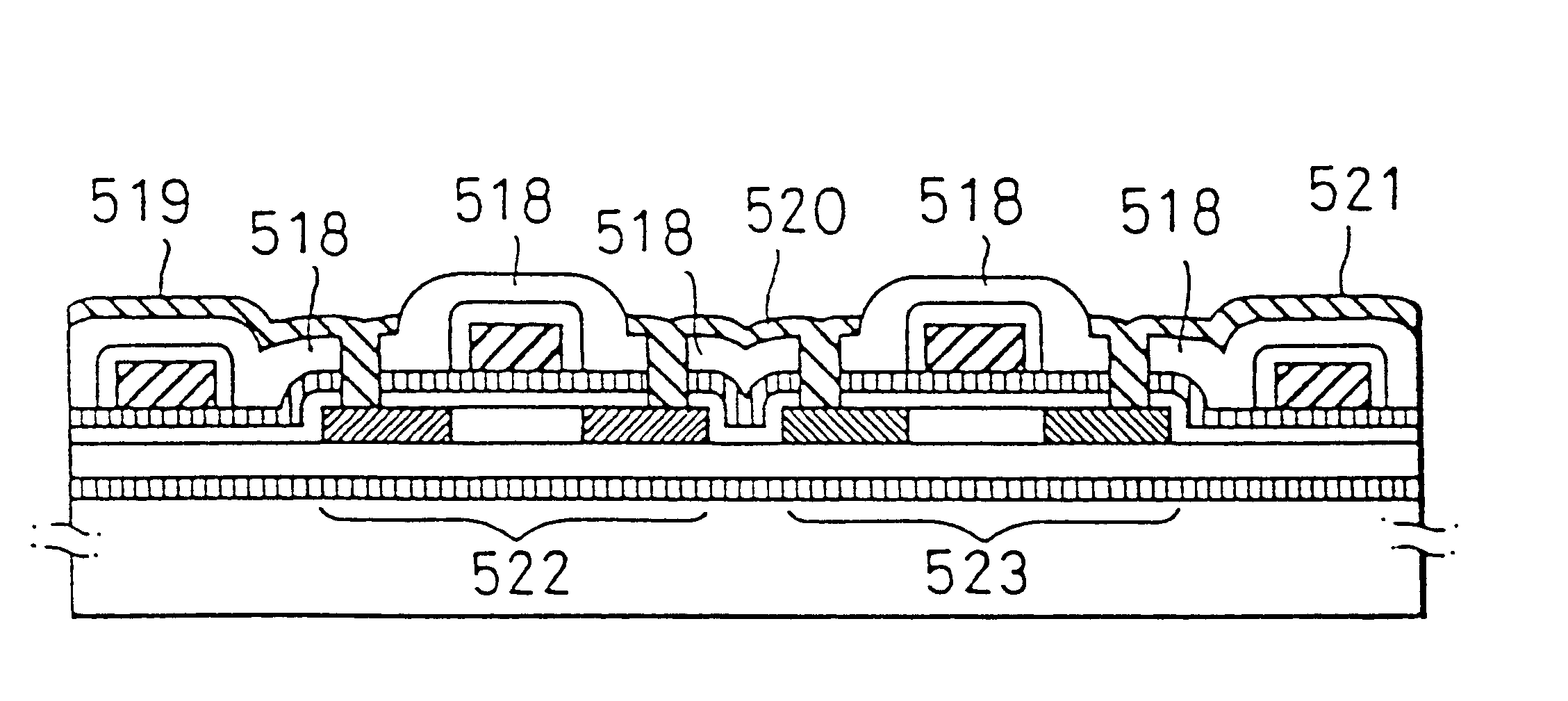
FIG. 2 shows an embodiment in which this invention was applied to a TFT having two-layered channel which was invented by the inventor of this application, et.al., and described in applications filed on Feb. 25, 1992 entitled "THIN FILM INSULATING GATE TYPE OF SEMICONDUCTOR DEVICE AND A PRODUCING METHOD THEREFOR" (applicant: Semiconductor Energy Laboratory Co., ?Ltd, docketing numbers: P002042-01 to P002044-03).

That is, in FIG. 2, a reference numeral 201 represents an N-channel TFT, a reference numeral 202 represents a P-channel TFT, and first layers 208 and 210 at these channel regions were substantially formed of amorphous silicon. The thickness thereof was set to 20 to 200 nm.

Reference numerals 207 and 209 represent silicon in a substantially polycrystal or semi-amorphous state, and the thickness thereof was set to 20 to 200 nm. Reference numerals 204 and 206 represent gate insulating films formed of silicon oxide, and the thickness thereof was set to 50 to 300 nm. Reference numer...

embodiment 3

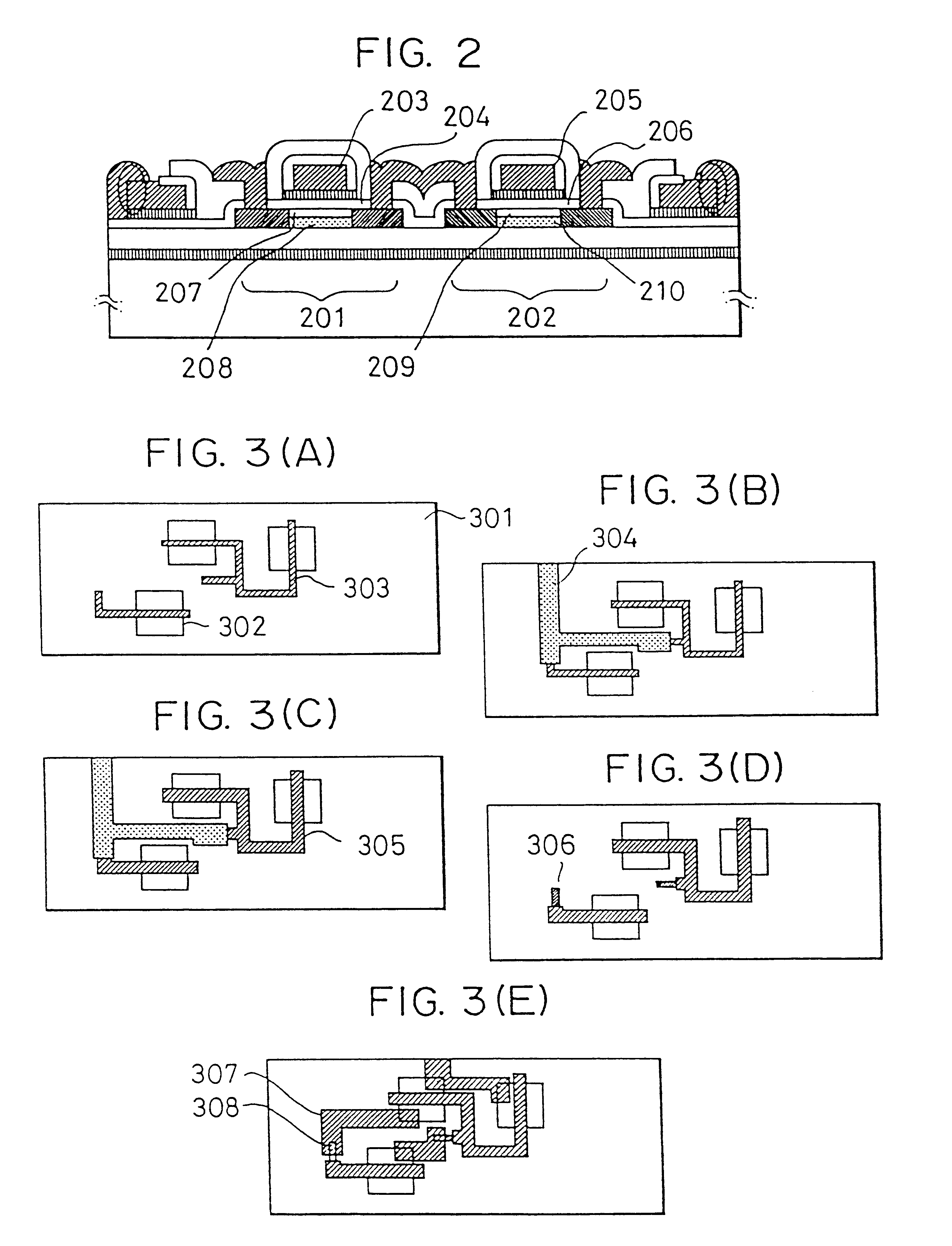
FIG. 3 shows a process for performing an anodic oxidation and then wiring using this invention. First, plural islandish semiconductor regions 302 were formed like the Embodiment 1, and a gate insulating film and a silicon nitride film of this invention (if occasion demands) were formed. Thereafter, aluminum gate electrode / wirings 303 were formed as a first conductor layer by patterning (FIG. 3(A)).

Subsequently, a wiring 304 for positive-electrode wiring was formed of chromium as a second conductor layer in contact with the gate electrode / wirings. The same condition for the chrome film as the Embodiment 1 was adopted (FIG. 3(B)).

Under the same condition as the Embodiment 1, the chrome wiring 304 was subjected to the anodic oxidation while kept to a positive potential, and an anodic oxide film 305 was formed on the surface of each gate electrode / wiring by making a current flow through the first conductor layer and the second conductor layer in an electrolyte. The oxide film 305 compri...


PUM


Abstract

In a thin-film insulated gate type field effect transistor having a metal gate in which the surface of the gate electrode is subjected to anodic oxidation, a silicon nitride film is provided so as to be interposed between the gate electrode and the gate insulating film to prevent invasion of movable ions into a channel, and also to prevent the breakdown of the gate insulating film due to a potential difference between the gate electrode and the channel region. By coating a specific portion of the gate electrode with metal material such as chrome or the like for the anodic oxidation, and then removing only the metal material such as chrome or the like together with the anodic oxide of the metal material such as chrome or the like, an exposed portion of metal gate (e.g. aluminum) is formed, and an upper wiring is connected to the exposed portion. Further, an aluminum oxide or silicon nitride is formed as an etching stopper between the gate electrode and the gate insulating film or between the substrate and the layer on the substrate, so that the over-etching can be prevented and the flatness of the element can be improved. In addition, a contact is formed in no consideration of the concept "contact hole".

Description

BACKGROUND OF THE INVENTION1. Field of the InventionThis invention relates to an insulated gate type semiconductor device, and particularly to the improvement of the structure of a thin-film insulated gate field effect transistor (TFT) and a method for producing the same.2. Description of Related ArtsRecently, a thin-film insulated gate field effect transistor (TFT) has been extensively studied. For example, in Japanese Patent Application No. 3-237100 or No. 3-238713 which has been invented by this inventor, et.al., are disclosed a TFT and a method of producing the same in which a gate electrode formed of aluminum is coated therearound with aluminum oxide which is formed by an anodic oxidation method, and a source / drain region is recrystallized by a laser annealing treatment.The TFT thus formed has been proved to have a more excellent characteristic in comparison with a conventional silicon gate TFT or a TFT having a gate electrode which is formed of metal having high melting point ...

Claims


Application Information

Patent Timeline
IPC IPC(8): H01L21/02H01L29/786H01L27/12H01L21/336H01L29/49H01L29/40H01L29/66H01L29/04
CPCH01L27/12H01L29/04H01L29/4908H01L29/66757H01L29/78666H01L29/78675H01L29/78696
Inventor YAMAZAKI, SHUNPEIZHANG, HONGYONGTAKEMURA, YASUHIKO
Owner SEMICON ENERGY LAB CO LTD
Why Eureka
Try Eureka