[0008]The present invention comprises
microelectromechanical systems (MEMS) actuated probe based memory technology in conjunction with a metal sulfide based
semiconductor film memory media. Areal density or the number of bits per square inch, in a probe-based
system is a function of probe size, probe resolution, and precision of actuation. The present invention provides tremendous improvements over conventional storage devices by optimizing each of these parameters, resulting in a high capacity, inexpensive, and extremely small non-
volatile memory device.
[0010]A metal sulfide based
memory cell that is programmed by means of impedance levels is advantageous in several ways. First, in contrast to
conventional memory cells that can only hold two bits of information (e.g., high or low), each metal sulfide based
memory cell is capable of holding a plurality of bits, because the conductive media of the
memory cell can have numerous impedance intensities (e.g., high, low, medium, very low, etc.). Therefore, the areal density of an array of memory cells is drastically increased at no additional cost. A further
advantage of metal sulfide based memory cells is that they have low power requirements, largely because they do not require a
constant power supply or refresh cycles to maintain the desired state like some conventional
random access memories (RAM). Additionally, the present invention provides metal sulfide based memory devices that possess at least one or more of the following: small size compared to inorganic memory devices, low cost, high reliability, long life, light weight, and
extended memory retention. Employing MEMS technology in conjunction with a metal sulfide based media provides still further advantages over
conventional memory devices.
[0011]MEMS technology enables integration of electrical and
mechanical components at a sub-
micron scale, which facilitates forming a memory device that is both extremely small and relatively inexpensive. The memory device of the present invention uses micro-fabricated components to reduce the scale and
power consumption of the memory device.
Power consumption is further reduced due in part to the use of rectilinear motion as opposed to more power hungry rotating medias (e.g., magnetic or optical disk). Additionally, because MEMS fabrication employs traditional
semiconductor processing technologies, the cost of manufacturing MEMS based memory devices is mitigated.
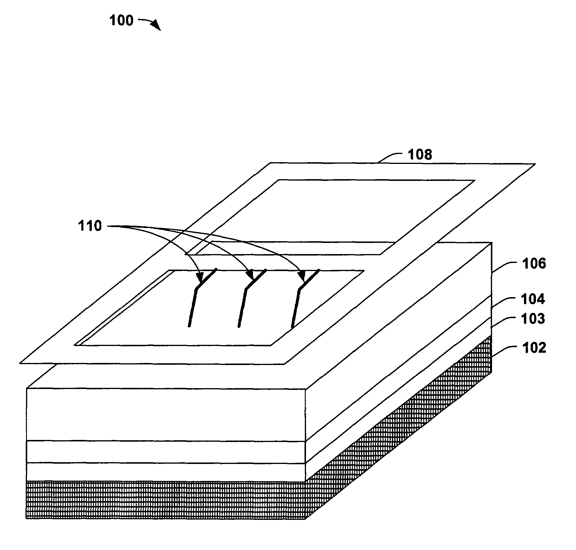
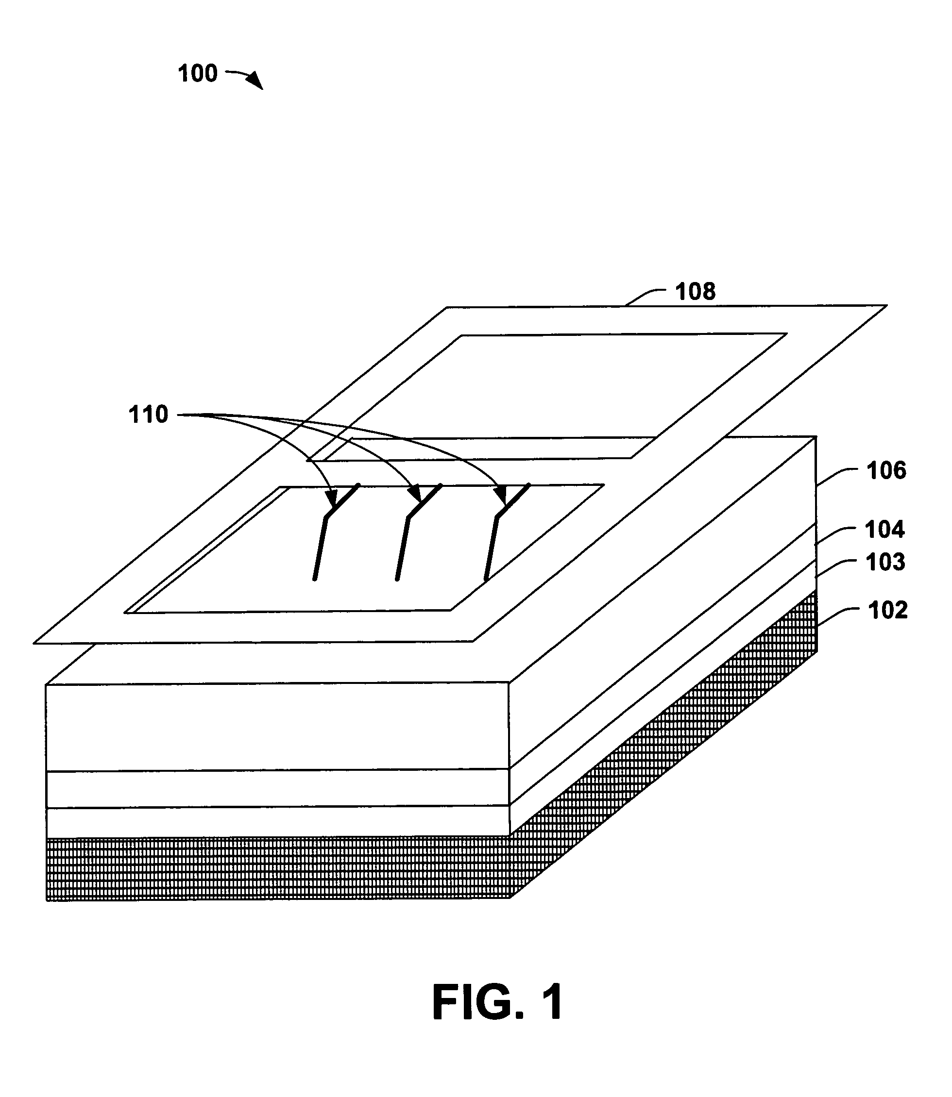
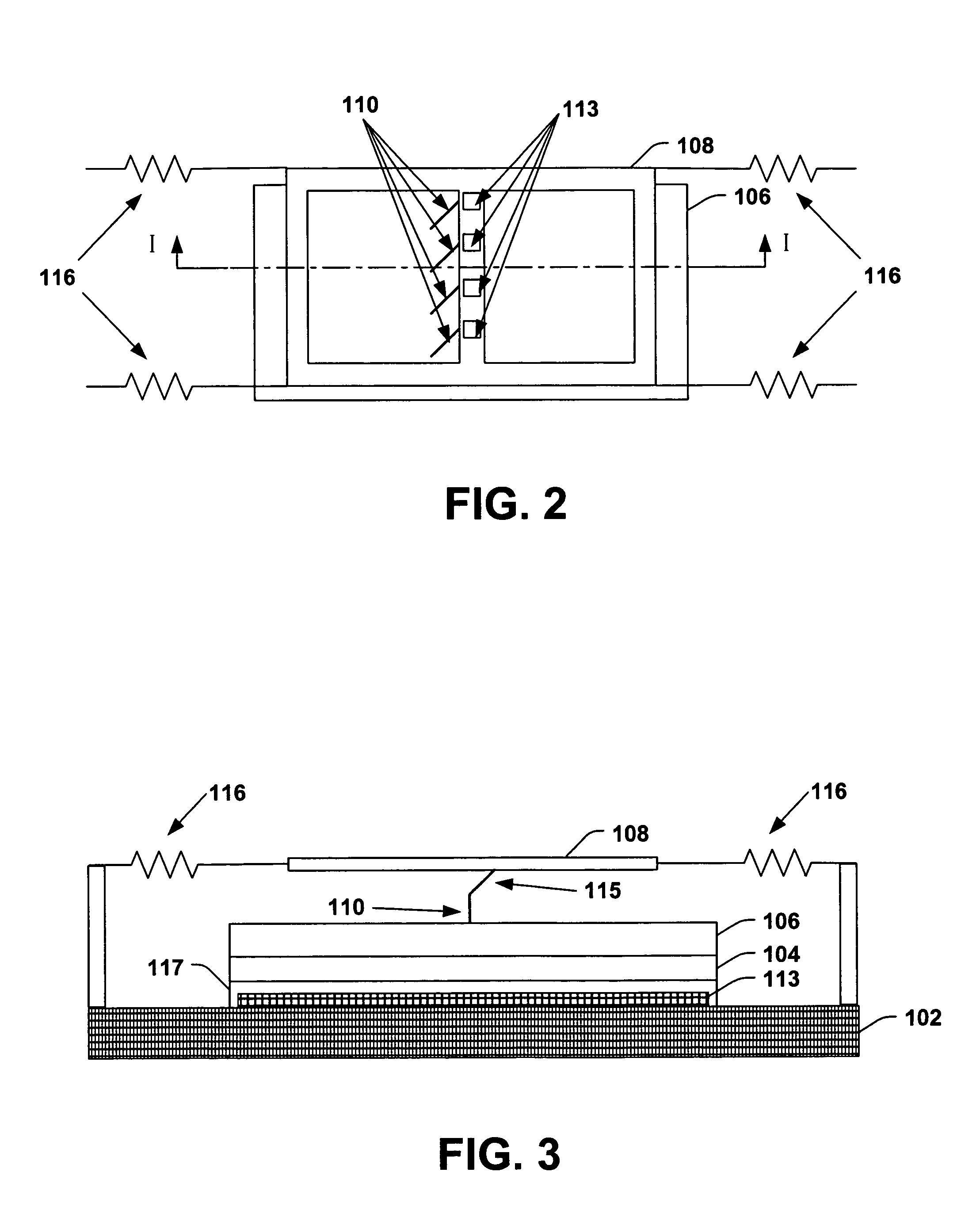
[0012]One embodiment of the present invention employs an array of MEMS probes to read, write, and erase metal sulfide based memory cells. Simple surface contacting probes or the more complex scanning tunneling probes may be used to provide nano-scale surface observation and memory
cell programming. Scanning tunneling probes operate using
quantum mechanical tunneling.
Quantum mechanical tunneling, or
tunnel current, can be induced by applying a bias
voltage between the probe and the memory
cell. The probe tips, being positioned very close to the media surface, are capable of detecting
tunnel current between the probe and the memory
cell, thereby allowing the
tunnel current to be measured and the impedance state of the memory cell to be determined. The foremost
advantage to using probes is their size. Traversing a memory device with
nanometer size probe tips that can sense forces at an atomic level allows the bits sizes of the media to be extremely small. However, bit size is also limited by the resolution of probe actuation.
[0013]A high precision mechanism is required in order to access multiple memory cells via probe actuation. MEMS actuators provide such positioning. Using different actuating technologies a MEMS actuator may deliver micro actuations of sub-micron to nano-level resolution. Besides the diminutive size, the MEMS actuation of the present invention is extremely accurate. One reason for such accuracy is that the probes may but are not required to maintain continuous contact with the surface. In contrast,
conventional memory devices that employ probes in constant contact with a media have problems with
static friction (“striction”), which prevents accurate positioning and thereby limits discernible
cell size. A further
advantage of the metal sulfide based memory medium in conjunction with a MEMS actuator is that the selection of the memory cell location does not involve a selection device, such as a
diode or
transistor, integrated with the cell. Selection is through location by the MEMS probes.
[0014]The present invention provides a considerable improvement over conventional
mass storage technologies by vastly increasing
data density. Employing atomic scale probes alone can significantly increases areal density by making distinguishable memory cell sizes many times smaller than conventional technologies (e.g.,
flash memory). When this increase in density is then combined with a multiple
cell state metal sulfide based media, the result is an extremely small, inexpensive, and low power ultra-
high density memory device.

