Method of manufacturing gate insulated field effect transistors

a gate-insulated field effect transistor and gate-insulated technology, applied in the direction of semiconductor devices, vacuum evaporation coatings, coatings, etc., can solve the problems of difficult to achieve uniform semiconductor film deposit by low pressure cvd, direct deposition of polycrystalline, and insatiable electric characteristics of hydrogenated amorphous semiconductors deposited by sputtering

Inactive Publication Date: 2009-03-24
SEMICON ENERGY LAB CO LTD
View PDF120 Cites 9 Cited by
  • Summary
  • Abstract
  • Description
  • Claims
  • Application Information

AI Technical Summary

Benefits of technology

[0022]In accordance with preferred embodiments, an oxide film forming a gate insulating film and a semiconductor film forming a channel region are deposited successively so that the electrical characteristics of the gate insulated field effect transistor formed

Problems solved by technology

Polycrystalline films are formed by depositing amorphous semiconductor films by low pressure CVD and then recrystallizing the amorphous films since direct deposition of polycrystalline films on wide areas is difficult for the reason of reaction temperature.
On the other hand, it is very difficult to deposit uniform semiconductor films by low pressure CVD.
This is the problem also in the case of plasma CVD whi

Method used


Image

  • Method of manufacturing gate insulated field effect transistors
  • Method of manufacturing gate insulated field effect transistors
  • Method of manufacturing gate insulated field effect transistors

Examples


first embodiment

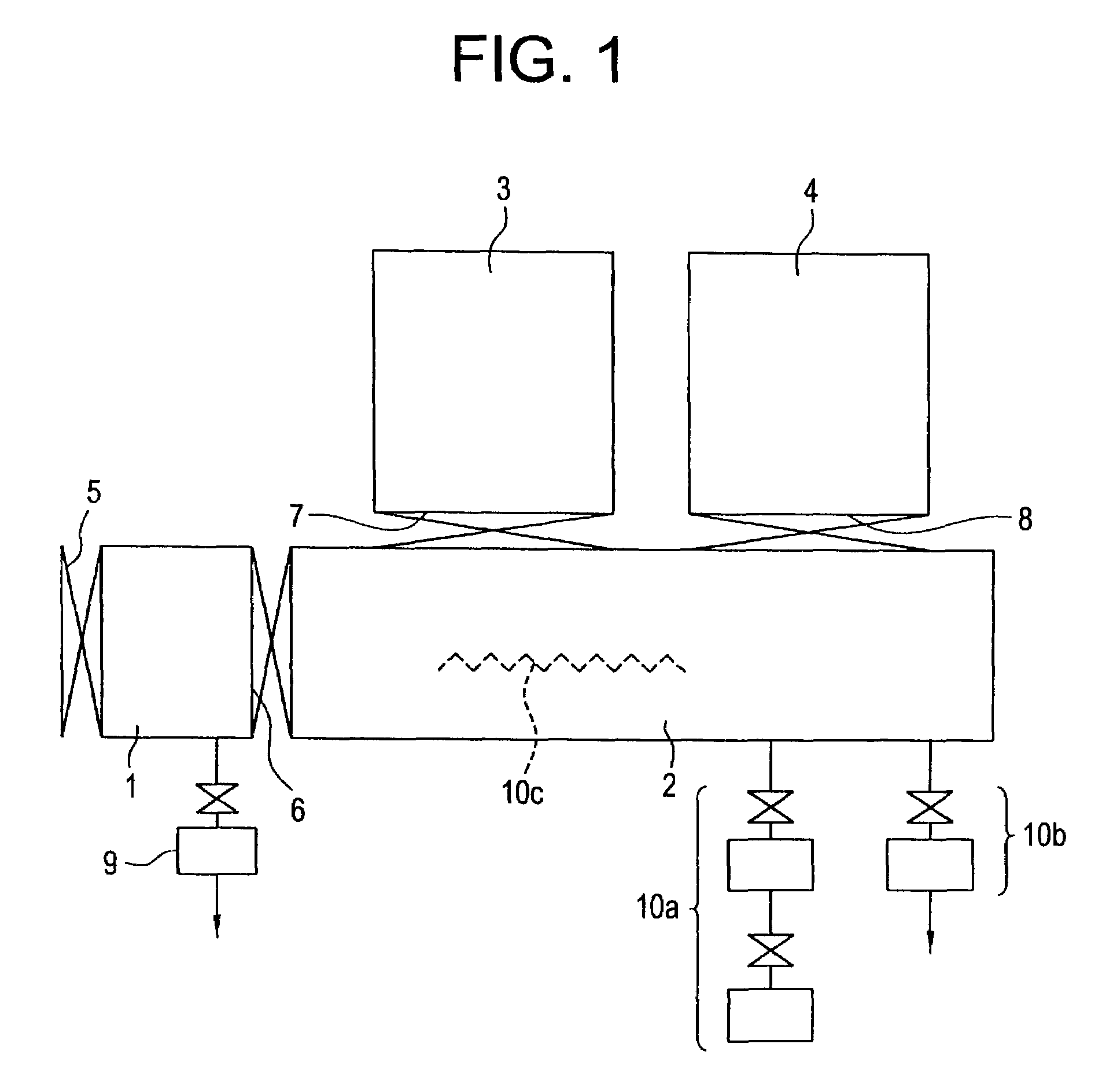
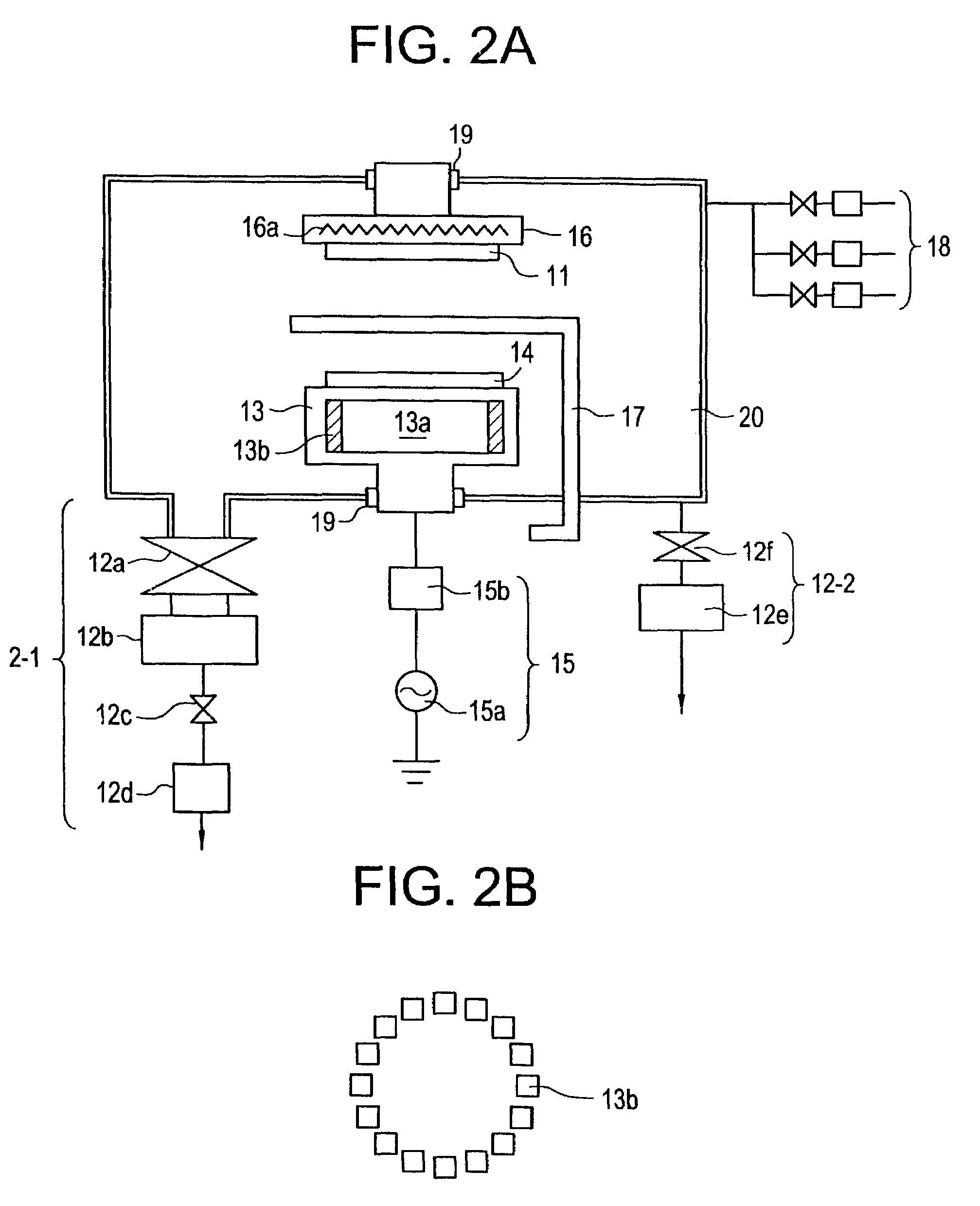
[0036]Referring now to FIG. 1, FIGS. 2(A) and 2(B) and FIGS. 3(A) to 3(D), a method of manufacturing gate insulated field effect transistors will be explained. FIG. 1 is a schematic view showing multi-chamber sputtering system for depositing semiconductor and gate insulation films by magnetron RF sputtering in accordance with the present invention. The system comprises a loading and unloading pre-chamber 1 provided with a gate valve 5, a subsidiary chamber 2 connected to the pre-chamber 1 through a valve 6 and first and second individual sputtering apparatuses 3 and 4 connected to the subsidiary chamber 2 respectively through valves 7 and 8. The pre-chamber 1 is provided with an evacuation system 9 comprising a rotary pump and a turbo molecular pump in series. The subsidiary chamber 2 is provided with a first evacuation system 10a for roughing comprising a rotary pump and a turbo molecular pump in series, a second evacuation system 10b for high vacuum evacuation comprising a cryosor...

second embodiment

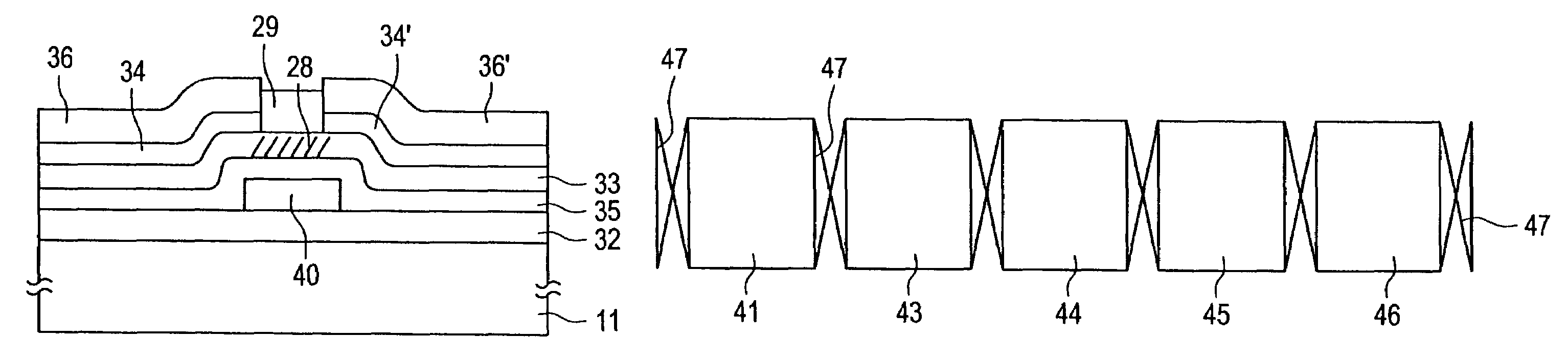
[0059]In accordance with the second embodiment, since the gate insulating film 35 is formed in advance of the formation of the semiconductor film 33 forming the channel 28, the interface between the insulating film 35 and the channel 28 is readily thermal annealed so that the density of surface levels can be decreased. The oxygen density in the semiconductor film 33 and the mobility were measured respectively to be 1×1019 cm−3 and 40.8 cm2 / Vsec.

[0060]Referring to FIG. 9 and FIGS. 10(A) to 10(E), a method of manufacturing gate insulated field effect transistors in accordance with a third embodiment of the present invention will be explained. FIG. 9 is a schematic view showing multi-chamber sputtering system for depositing semiconductor and oxide films by magnetron RF sputtering. The system comprises a loading prechamber 41, first, second and third individual sputtering apparatuses 43, 44 and 45 and an unloading chamber 46. These chambers and sputtering apparatuses are connected in se...

third embodiment

[0066]The above explanation of the third embodiment has been carried out successively following the treatment of one substrate. The manufacturing process, however, is carried out in a pipeline fashion. Each sputtering apparatus receives a next substrate when a preceding substrate is coated and transported to the right-side sputtering apparatus or the unloading chamber 46, and carries out deposition on the next substrate concurrently with the other apparatuses unless deposition on all the 10 substrates has been finished. Needless to say, the transportation of each substrate between adjacent two of the loading chamber 41, the sputtering apparatuses 43, 44 and 45 and the unloading chamber 46 is carried out after adjusting the pressures and the inner atmospheres of the two in order not to eliminate undesirable impurities as explained in the foregoing embodiment.

[0067]After all the substrates are coated with the silicon oxide and amorphous silicon semiconductor film 32, 33 and 35 and col...


PUM

PropertyMeasurementUnit
Temperatureaaaaaaaaaa
Areaaaaaaaaaaa
Diameteraaaaaaaaaa

Abstract

A method of manufacturing thin film field effect transistors is described. The channel region of the transistors is formed by depositing an amorphous semiconductor film in a first sputtering apparatus followed by thermal treatment for converting the amorphous phase to a polycrystalline phase. The gate insulating film is formed by depositing an oxide film in a second sputtering apparatus connected to the first apparatus through a gate valve. The sputtering for the deposition of the amorphous semiconductor film is carried out in an atmosphere comprising hydrogen in order to introduce hydrogen into the amorphous semiconductor film. On the other hand the gate insulating oxide film is deposited by sputtering in an atmosphere comprising oxygen.

Description

[0001]This application is a Divisional of prior application Ser. No. 09 / 877,059, filed Jun. 11, 2001, now, U.S. Pat. No. 6,566,175; which itself is a Divisional of application Ser. No. 08 / 677,331, filed Jul. 2, 1996, now U.S. Pat. No. 6,261,877; which itself is a Divisional of Ser. No. 08 / 310,364, filed Sep. 22, 1994, now U.S. Pat. No. 6,177,302; which itself is a Continuation of application Ser. No. 07 / 673,417, filed Mar. 22, 1991, now abandoned.BACKGROUND OF THE INVENTION[0002]1. Field of the Invention[0003]The present invention relates to a method of manufacturing semiconductor devices and, more particularly to a method of manufacturing thin film gate insulated field effect transistors consisting of polycrystalline semiconductor films.[0004]2. Description of the Prior Art[0005]The prior art includes methods utilizing low pressure CVD by which polycrystalline semiconductor thin films are deposited at temperatures ranging from 550° C. to 900° C. Recently, along with development of ...

Claims


Application Information

Patent Timeline
IPC IPC(8): H01L21/84C23C14/56H01L21/20H01L21/203H01L21/336
CPCC23C14/568H01L29/66757H01L21/02422H01L21/02488H01L21/02532H01L21/02631H01L21/02661Y10S438/906Y10S438/907Y10S438/908
Inventor YAMAZAKI, SHUNPEIZHANG, HONGYONGINUSHIMA, TAKASHIFUKADA, TAKESHI
Owner SEMICON ENERGY LAB CO LTD
Why Eureka
Try Eureka