Method of manufacturing LCD apparatus by using halftone exposure method

a technology of liquid crystal display and exposure method, which is applied in the direction of instruments, semiconductor devices, optics, etc., can solve the problems of abnormal etching, reduced transparent electroconductive film, and melted particles at the substrate surfa

Inactive Publication Date: 2009-10-13
MIKUNI ELECTORON CO LTD
View PDF20 Cites 33 Cited by
  • Summary
  • Abstract
  • Description
  • Claims
  • Application Information

AI Technical Summary

Benefits of technology

[0302]Measures 1 to 16 are used for manufacturing a thin film transistor matrix substrate to reduce the mask manufacturing process as shown in FIGS. 36, 169 and 212, a thin film transistor component (68) of a static charge protection circuit is formed at the periphery of a display region and on the thin film transistor matrix substrate. In FIG. 169, the static charge protection circuit adopts an electrode made of the same material of a common electrode (65), a gate electrode (13) and a source electrode (29). Even if a static charge of a large capacitor is introduced, the electrodes will not be heated up or melted. For a static charge protection circuit made of transparent thin film electrode material such as a pixel electrode, the contact resistance is high, and thus having a heating and melting issue.
[0303]For Measures 1 to 16, the pixel electrode can be made of titanium, zirconium, a metal nitride of the above, or an oxygen nitride. The manufacturing process of FIGS. 84 to 86 is used for separating the thin film semiconductor component of FIG. 85 and etching and removing the semiconductor layer and gate insulating film (P—SiNx) on the pixel electrode by using a fluorine-series gas dry etching method. In the foregoing manufacturing process, the pixel electrode cannot be one made of titanium or zirconium nitride or oxygen nitride, since the dry etching selection ratio of titanium or zirconium nitride or oxygen nitride and the gate insulating film (P—SiNx) is low. If Measures 1˜16 as shown in FIGS. 3, 4, 5, 8, 9, 27, 28 and 29 are used, a contact pad portion (9) is formed in a pixel electrode portion. If the contact pad portion is made of aluminum alloy, the dry etching selection ratio of the gate insulating film (P—SiNx) is higher, and thus the pixel electrode can be made of titanium, zirconium, a metal nitride of the above, or an oxygen nitride with a thin thickness of 5 nm˜15 nm. Similar to the description of Measures 1˜16, a contact pad is formed inside the pixel electrode, for protecting the 5˜15 nm thin film of titanium nitride or zirconium nitride, and allowing the formation of a contact hole, and thus no ITO or IZO transparent electroconductive film is required in the pixel electrode, and the low-cost titanium or zirconium can be used for spluttering. In FIG. 10, the 5˜10 nm titanium nitride thin film provides a light transmission rate of over 80% in the visible light region. In FIG. 11, the 5˜10 nm titanium nitride thin film has a surface electric resistance below 30 KΩ, and it can be used as a transparent pixel electrode.
[0304]For Measure 17, 18, 20, 21, 23, 24, 26 or 27, abnormal electric discharges occurred in the process of sintering an ITO or IZO metal oxide powder can be reduced significantly since a metal with a low melting point such as titanium or zirconium is used, and thus the yield rate can be improved. The surface of the ITO or IZO conductor film is very rough. The surface will become rougher after a metal film is formed, and thus short circuit occurs easily at the ITO or IZO gate electrode and the source electrode short circuit, and the static charge resistance will be lowered. The surface of a film formed by sputtering with titanium or zirconium metal will be very fine and smooth like a mirror. Therefore, the chance of having a short circuit at the gate electrode and the source electrode will be lowered, and thus improving the yield rate.
[0305]In Measures 17, 18, 19, 20, 21, 22, 23, 24, 25, 26, 27, 28, 33, 34, 35 and 36, the ITO and aluminum alloy seldom has a chemical reaction such as a local cell reaction. Even if both gate electrode and pixel electrode are formed on the same layer, no abnormal etching reaction will occur. In the aforementioned manufacturing process as shown in FIGS. 84 to 86, if the pixel electrode is exposed completely exposed, aluminum alloy cannot be used in the source electrode or the drain electrode, and large LCD panels cannot be manufactured. In the present invention, a contact pad is formed on the ITO transparent pixel electrode, and if the transparent pixel electrode except the contact hole is completely covered by the gate insulating film, the occurrence of chemical reaction such as local cell reaction still can be suppressed regardless of the types of electrode material used for the source electrode and the drain electrode.
[0306]With doped nitrogen atoms in a region of a second layer (or upper layer) metal of the first film formation used in Measures 29 and 30 as shown in FIG. 122, the halftone exposure manufacturing process as shown in FIGS. 112 to 114 can be used for manufacturing the second layer (or upper layer) metal into a regular conical shape. If the regular conical shape cannot be achieved, defects like wire breaking at the source electrode or the drain electrode and short circuits at the gate electrode and the source electrode or the drain electrode will occur easily, and thus lowering the yield rate. With the present invention, the etching speed for a two-layer interface can be controlled to prevent a drop of yield rate, even if a first layer (or lower layer) metal or a first layer (or lower layer) thin film transparent conductor is stacked with a second layer (or upper layer) metal.
[0307]In Measures 17, 18, 19, 20, 21, 22, 23, 26, 31 and 32, after a contact hole is formed on the gate electrode made of aluminum alloy, and a positive photoresist is formed by ashing of the halftone manufacturing process for suppressing the oxidation of the aluminum alloy surface. After a pattern is produced in accordance with the present invention, nitrogen ions are implanted on the aluminum alloy surface by an ion doping device. Unlike the method disclosed in Japanese Patent Laid-Open Publication No. 2001-174848 that an aluminum alloy film is formed by spluttering, and a mixed nitrified gas and argon inert gas are used for performing reaction and spluttering, and nitrogen atoms are doped on the aluminum alloy surface, the present invention does not form an inverted conical shape structure. In the conventional anti-oxidation treatment of the aluminum alloy surface, the aluminum alloy pattern as shown in FIG. 105 will be formed. In the present invention as shown in FIGS. 1, 2, 42, 43, 106, 112, 113, 114 and 176, a surface nitrification treatment can be performed even to the sidewalls of the aluminum alloy pattern, since the whole region of the substrate is reacted with a uniform concentration, and the surface nitrification treatment can be carried out to produce uniform depth, and thus having the advantages of a very good recurrence and a regular conical shape. In the conventional oxidation-resisting method for the aluminum alloy, it is very difficult to carry out nitrification evenly on the entire surface of the substrate, and an inverted conical shape etched form will result easily. In mass production, wire breaking may occurs at the source electrode or the drain electrode easily, and thus such prior art cannot avoid a reduction of the yield rate.

Problems solved by technology

Sintered powder particles of oxides such as ITO and IZO are used, since the insulating oxide formed at a target surface or an attachment-proof board surface may have abnormal electric discharges.
If the gate electrode so produced has abnormal electric discharges, the particles at the substrate surface will be melted by overburning, and the particles are washed away during the washing and cleaning process.
If the metal film is made of aluminum alloy, and the oxide transparent electroconductive film has a local cell reaction, the oxide transparent electroconductive film is reduced and blackened, and an abnormal etching is resulted.
Such reaction cannot be avoided in the manufacture that adopts the wet etching method, but the manufacture that adopts a dry etching method takes a relatively long manufacturing time, and causes corrosions when exposed in the atmosphere.
Molybdenum, chromium, or molybdenum tantalum film has high electric resistance, and thus these films cannot be used for producing a large LCD TV of over 30 inches.
Even if the electrodes are not made of a single-layer aluminum alloy, but the aluminum alloy film is formed on a barrier metal layer of molybdenum or chromium, the local cell reaction will occur during image development since the barrier metal layer has pin holes, and thus the occurrence of abnormal etching cannot be controlled completely.

Method used


Image

  • Method of manufacturing LCD apparatus by using halftone exposure method
  • Method of manufacturing LCD apparatus by using halftone exposure method
  • Method of manufacturing LCD apparatus by using halftone exposure method

Examples


embodiment 1

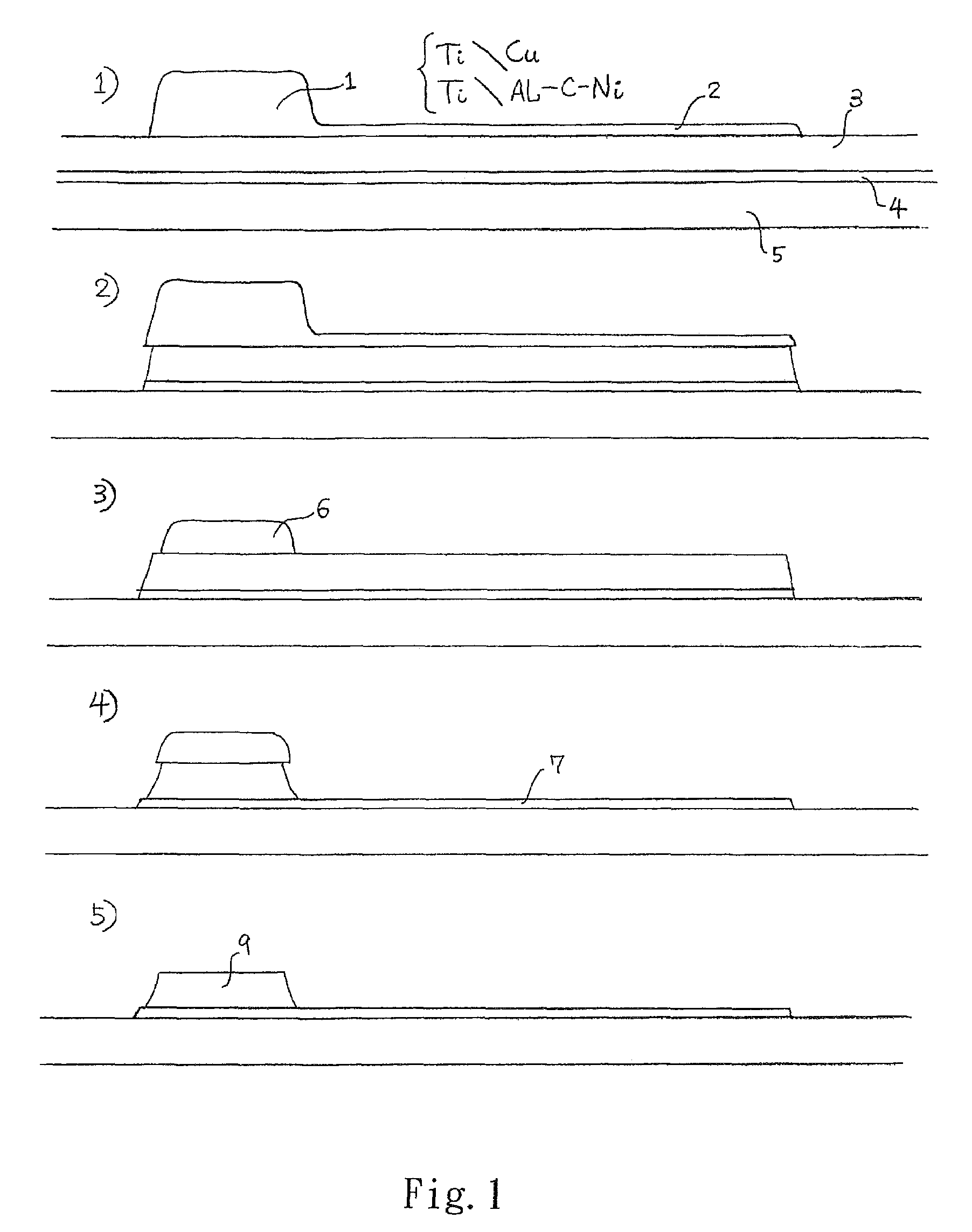
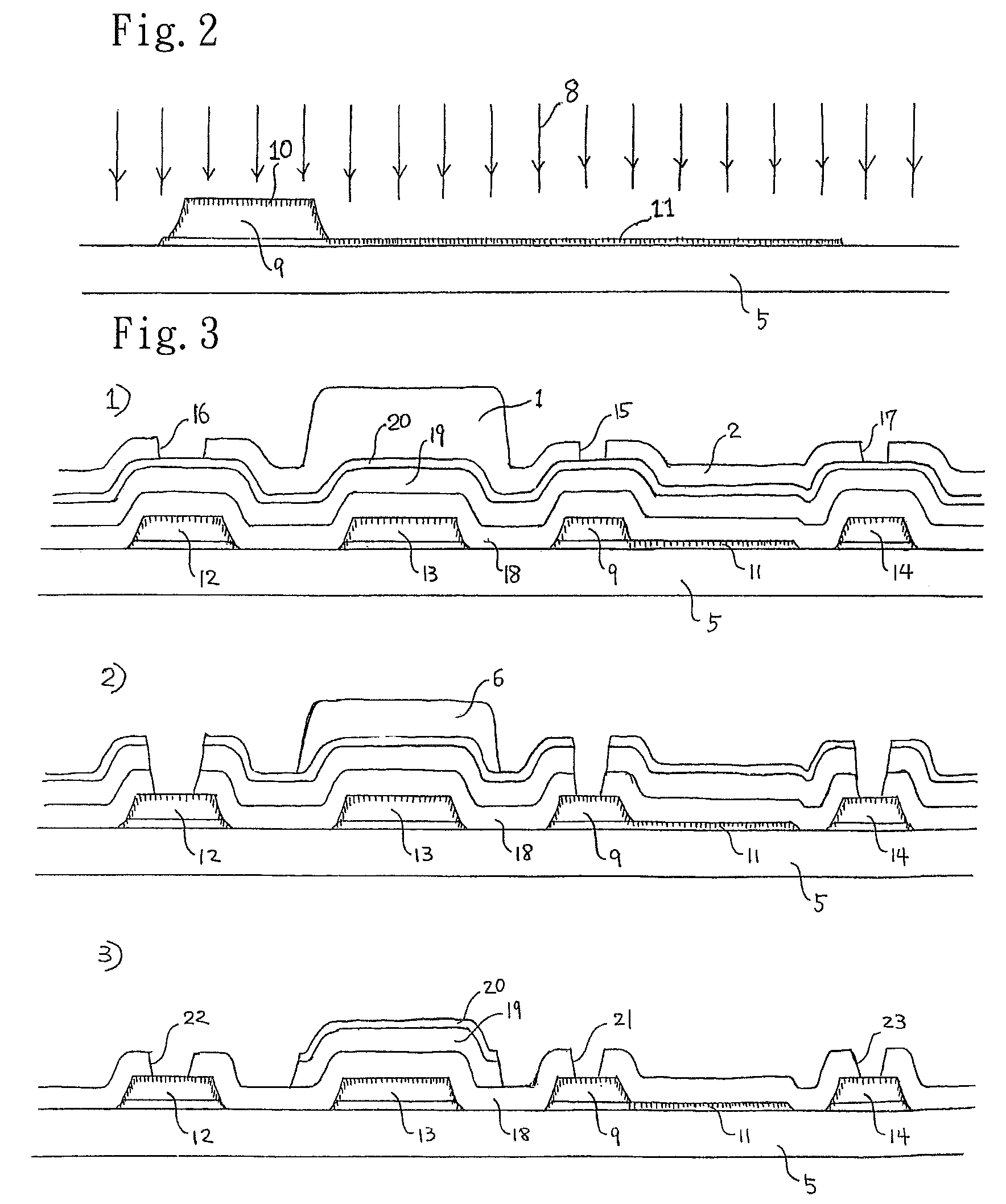
[0641]Referring to FIGS. 11 to 15 for a schematic cross-sectional view of a manufacturing process of an active matrix TFT substrate in accordance with Embodiment 1 of the present invention, a titanium thin film or a zirconium thin film of 5˜25 nm is formed on a glass substrate, and then an aluminum alloy (aluminum-carbon-nickel or aluminum-neodymium-nickel), copper or copper alloy (copper-nickel or copper-chromium) or silver alloy of 200˜800 nm is formed on the whole surface of the substrate as shown in FIGS. 249 and 250. After the positive photoresist is coated, a halftone exposure method is used for carrying out an exposure to develop an image and produce a positive photoresist pattern in the shape as shown in FIG. 1-1. In FIG. 1-2, the pattern is used for simultaneously etching and manufacturing a lower layer metal thin film and an upper layer metal thin film into the same shape, and then an oxygen plasma ashing process is used for ashing away the thin positive photoresist region...

embodiment 2

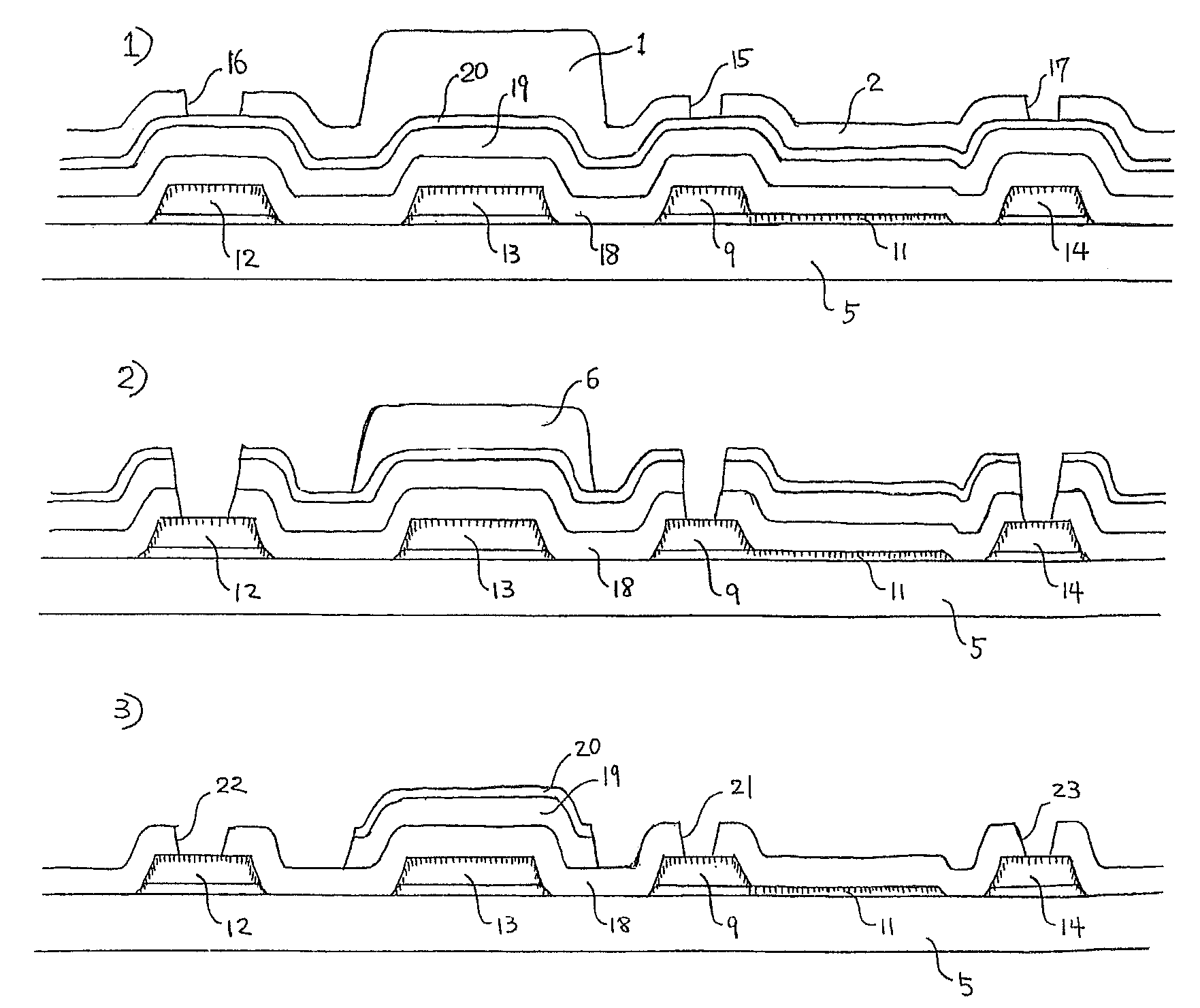
[0648]FIG. 248 shows a schematic cross-sectional view of a manufacturing process for forming a pixel electrode by using the halftone exposure method in accordance with Embodiment 2 of the present invention. As shown in FIG. 1-2, two metal films are etched and manufactured to a same pattern. Embodiment 2 of the present invention is shown in FIG. 248-2. Firstly, a metal film of an upper layer is etched selectively as shown in FIG. 248-3, and after an oxygen plasma ashing process is performed to remove the region of a thin positive photoresist left from a halftone exposure, a metal pattern of the upper layer serves as a mask, and the dry etched metal thin film of the lower layer is patterned. After the upper layer metal is selectively etched and exposed, a nitrogen ion shower doping process is performed, and the nitrogen atoms doped on the metal surface of the upper layer of a contact pad portion to provide an oxidation-resisting function. In the meantime, the metal thin film pixel ele...

embodiment 3

[0650]FIG. 42 shows the cross-sectional view of a manufacturing process of forming a pixel electrode and a contact pad by using a halftone exposure method in accordance with Embodiment 3 of the present invention. This manufacturing process is classified as Type (IIa) manufacturing process as shown in FIG. 46. Aluminum alloy (aluminum-carbon-nickel or aluminum-neodymium-nickel), pure copper, copper alloy (copper-molybdenum or copper-chromium) or silver alloy (silver-copper or silver-palladium) that does not cause Hirox is used as the upper layer metal. The gate electrode and the common electrode of a super large TFT matrix substrate for LCD TV adopt the metal of the aforementioned three systems. The lower layer transparent conducting electrode of the present invention adopts titanium nitride or zirconium nitride, for the reason of: the aforementioned two types of nitride material and aluminum alloy do not cause a local cell reaction (or a Galvanic reaction). Furthermore, both wet etc...


PUM

PropertyMeasurementUnit
thicknessaaaaaaaaaa
thicknessaaaaaaaaaa
thicknessaaaaaaaaaa

Abstract

The present invention discloses a method of manufacturing a super large wide-angle super high-speed response LCD apparatus by using a photolithographic process for three times. The invention adopts a halftone exposure technology and a nitrogen ion doped technology to form a gate electrode, a common electrode, a pixel electrode and a contact pad, and then uses the halftone exposure technology to form a silicon (Si) island and a contact hole, and a general exposure technology to form a source electrode, a drain electrode and an alignment control electrode. A P-CVD apparatus is provided for forming a passivation layer into a film by using a masking deposition method, or an ink-jet coating method is used to coat a protective layer at a partial area, and a photolithographic process is performed for three times to manufacture a TFT matrix substrate of the super large wide-angle super high-speed response LCD.

Description

FIELD OF THE INVENTION[0001]The present invention relates to a method of manufacturing an active matrix substrate of a liquid crystal display by using a halftone exposure method.BACKGROUND OF THE INVENTION[0002]Mask is used for the halftone exposure of three regions: a complete UV photo interrupt region, an UV light semi-transmitting region and a complete UV light transmitting region to carry out a photolithographic process and produce positive photoresists of different thicknesses, and its related technologies have been disclosed in Japanese Patent Laid-Open Publication No. Sho-61-181130 (published on Aug. 13, 1986) and Japanese Patent Laid-Open Publication No. 10-163174 (published on Jun. 19, 1998). The mask used for the halftone exposure that reduces the number of times of the photolithographic process in a TFT matrix substrate manufacturing process has been disclosed in Japanese Patent Laid-Open Publication No. 2000-066240 (published on Mar. 3, 2000) and Japanese Patent Laid-Ope...

Claims


Application Information

Patent Timeline
Patent Type & Authority Patents(United States)
IPC IPC(8): G02F1/136
CPCG02F1/13458H01L27/1288H01L27/124G02F2001/136236G02F1/136236G02F1/1333G02F1/1362G02F1/13625G02F1/136
Inventor TANAKA, SAKAESAMEJIMA, TOSHIYUKI
Owner MIKUNI ELECTORON CO LTD
Why Eureka
Try Eureka