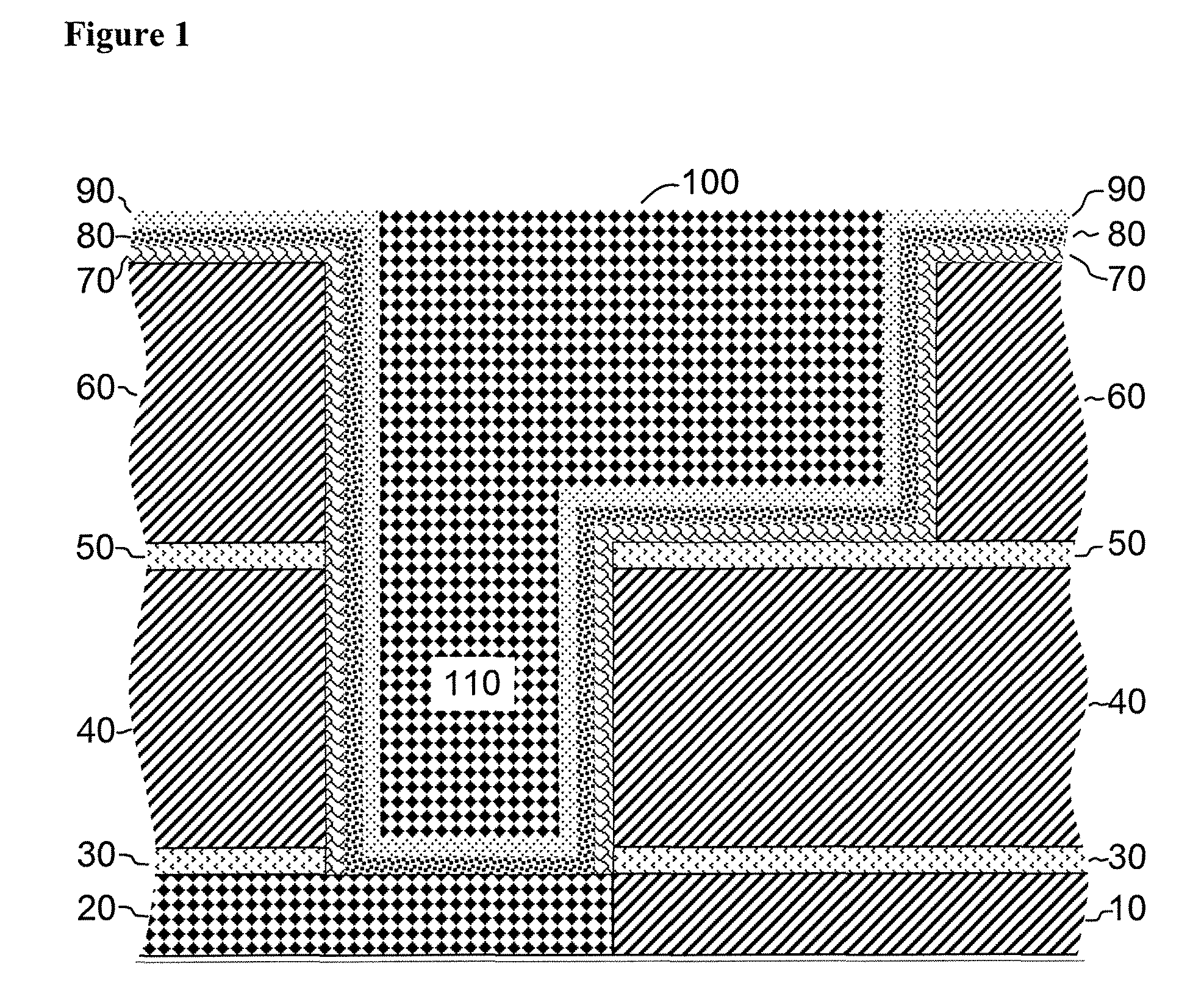
Cobalt nitride layers for copper interconnects and methods for forming them
a technology of copper nitride and copper interconnect, which is applied in the direction of resistive material coating, solid state diffusion coating, group 5/15 element organic compounds, etc., can solve the problems of copper increasing the leakage of current through insulators, preventing the proper functioning of transistors formed in semiconductors, and most of the unwanted motion occurs
- Summary
- Abstract
- Description
- Claims
- Application Information
AI Technical Summary
Benefits of technology
Problems solved by technology
Method used
Image

Examples
example 1
CVD of WN, Co4N and Cu
[0071]A silicon wafer with a SiO2 insulating layer on top was used as the substrate. Trenches and holes were etched in some areas of the SiO2 layer.
[0072]Tungsten nitride was deposited by CVD by exposing a vapor mixture of about 0.05 Torr bis(tert-butylimido)bis(dimethylamido)tungsten(VI), 0.5 Torr ammonia and 0.5 Torr nitrogen to a substrate temperature of 390° C. for 1 minute. A diffusion barrier of WN about 2 nm thick was deposited.
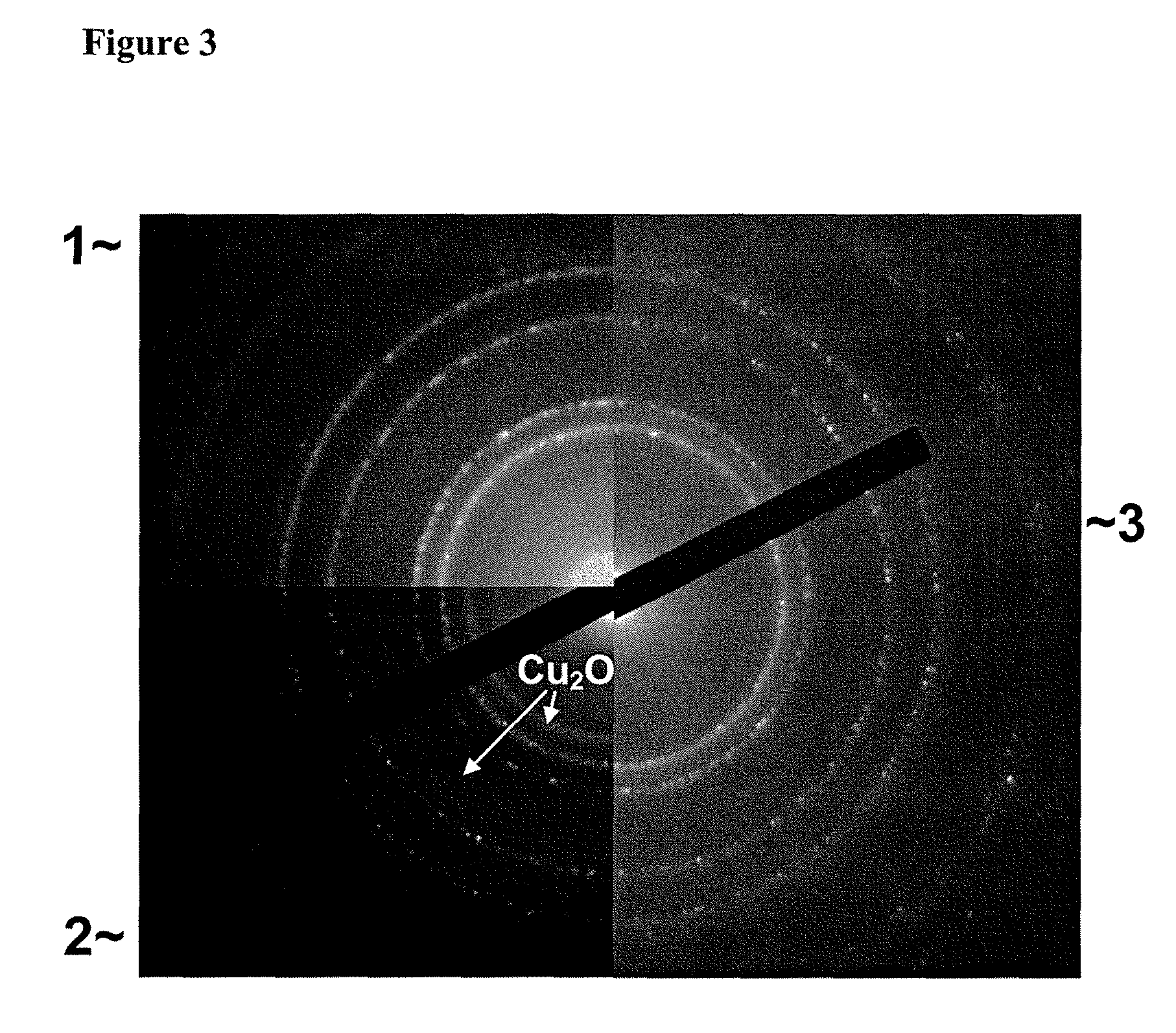
[0073]Cobalt nitride was deposited by CVD a vapor mixture of about 0.03 Torr bis(N-tert-butyl-N′-ethyl-propionamidinato)cobalt(II), 0.2 Torr ammonia, 0.3 Torr hydrogen and 0.5 torr nitrogen to a substrate temperature of 186° C. for 4 minutes. A layer comprising CoxN about 2 nm thick was deposited. For analysis of this CoxN material, thicker layers were deposited onto glassy carbon substrates and then subjected to Rutherford Backscattering Analysis (RBS). Cobalt and nitrogen were detected in the film with an atomic ratio x˜4, along...
example 2
CVD of WN, Co4N+CO3N and Cu
[0078]Example 1 is repeated except that during the CoxN deposition, 0.3 Torr ammonia, 0.2 Torr hydrogen was used. The deposition was carried out for 4 minutes, which was long enough to produce a CoxN layer about 2 nm thick. RBS analysis on a thicker film produced under the same conditions determined that the cobalt to nitrogen ratio x was between 3 and 4. Electron diffraction confirmed that the major phase of this film is Co4N, along with some hexagonal Co3N.
[0079]After deposition of the copper seed layer, the sheet resistance was about 2.4 times higher than the layers produced in Example 1. This example shows that a CO3N+Co4N mixture produces a more conductive copper film than pure Co, but not as pure conductive as Co4N does.
example 3
CVD of WN, CO3N and Cu
[0080]Example 1 is repeated except that during the CoxN deposition, 0.5 Torr of ammonia was used and no hydrogen was used. The deposition was carried out for 4 minutes, which was long enough to produce a CoxN layer about 2 nm thick. RBS analysis on a thicker film produced under the same conditions determined that the cobalt to nitrogen ratio x was approximately 3. Electron diffraction confirmed that the structure of the film was hexagonal Co3N.
[0081]After deposition of the copper seed layer, the sheet resistance was about 4 times higher than the layers produced in Example 1. This example shows that Co3N produces a more conductive film than pure Co, but not as conductive as Co4N does.
PUM
| Property | Measurement | Unit |
|---|---|---|
| RMS roughness | aaaaa | aaaaa |
| RMS roughness | aaaaa | aaaaa |
| temperature | aaaaa | aaaaa |
Abstract
Description
Claims
Application Information