

Ultraviolet nanoimprint resist and components thereof
A nano-imprinting and resist technology, applied in optics, opto-mechanical equipment, instruments, etc., can solve the problem of increasing environmental pollution and the harshness of the glue-sweeping process, the inability to achieve high-fidelity graphics transfer, and unfavorable promotion and application of imprinting technology, etc. problems, to achieve the effect of ensuring true transfer, low shrinkage and high repeatability
- Summary
- Abstract
- Description
- Claims
- Application Information
AI Technical Summary
Problems solved by technology
Method used
Image

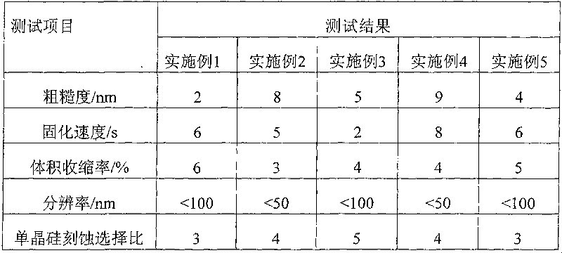
Examples
Embodiment 1
[0038] A resist for UV nanoimprinting was produced by combining the following ingredients.
[0039] Prepolymer: hyperbranched polyester acrylate (SARTOMER, CN2301), 10 parts
[0040] Aromatic monoacrylate (SARTOMER, CN131), 60 parts
[0041]Polyurethane acrylate (SARTOMER, CN963B80), 5 parts
[0042] Monomer: Isobornyl Methacrylate, 10 parts
[0043] Dipropylene glycol diacrylate, 10 parts
[0044] Photoinitiator: 1-Hydroxy-cyclohexyl-phenylmethanone, 2 parts
[0045] 2-Hydroxy-2-methyl-1-phenylpropanone, 2 parts
[0046] Additive: ethoxylated nonionic fluorosurfactant (Dupont, FSO-100), 1 part
Embodiment 2
[0048] A resist for UV nanoimprinting was produced by combining the following ingredients.
[0049] Prepolymer: epoxy acrylate (CYTEC, EBECRYL 9626), 10 parts
[0050] Aliphatic urethane triacrylate (CYTEC, EBECRYL 9260), 60
[0051] share
[0052] Monomer: 2-phenoxyethyl methacrylate, 15 parts
[0053] 1,3-Butanediol diacrylate, 10 parts
[0054] Photoinitiator: 2-phenylbenzyl-2-dimethylamine-1-(4-morpholinebenzylphenyl) butanone, 3 parts
[0055] Auxiliary agent: fluorine-containing nonionic surfactant (HENSIC, H-6910), 2 parts
Embodiment 3
[0057] A resist for UV nanoimprinting was produced by combining the following ingredients.
[0058] Prepolymer: aromatic epoxy acrylate (COGNIS, PHOTOMER 3016-25T F), 7 parts
[0059] Epoxy acrylate (COGNIS, PHOTOMER 3016-40RF), 55 parts
[0060] Monomer: Ethoxylated nonylphenol acrylate, 14 parts
[0061] 1,6-Hexanediol diacrylate, 14 parts
[0062] Photoinitiator: 2-methyl-1-[4-(methylthio)phenyl]-2-(4-morpholinyl)-1-propanone, 6 parts
[0063] Auxiliary: fluorocarbon modified polyacrylate (CIBA, EFKA3277), 4 parts
PUM
 Abstract
Description
Claims
Application Information