Preparation method of solar cell

A technology for solar cells and electrodes, applied in circuits, electrical components, and final product manufacturing, etc., can solve the problems of large leakage current, difficult to control the uniformity of corrosion tank parameters, and large damage to devices, and achieves improved parallel resistance and open circuit voltage. The effect of overcoming plasma bombardment damage and high conversion efficiency

Inactive Publication Date: 2011-01-05
百力达太阳能股份有限公司
View PDF5 Cites 31 Cited by
  • Summary
  • Abstract
  • Description
  • Claims
  • Application Information

AI Technical Summary

Problems solved by technology

However, dry etching has a poor etching selectivity ratio for the underlying material, and plasma etching is often accompanied by ion bombardment and radiation, and these phenomena will cause great damage to the device.
In addition, reaction residues are often deposited on the edge of the wafer leading to particle contamination and defects
These will seriously affect the stability of etching, affect the electrical performance of the product, and cause the parallel resistance of the battery sheet to be small and the leakage curre

Method used


Image

  • Preparation method of solar cell
  • Preparation method of solar cell
  • Preparation method of solar cell

Examples


Embodiment 1

[0038] Figure 1a Structural schematic diagram of the tubular machine used in the present invention; Figure 2a ~ Figure 2f Process flow chart for the preparation of solar cells of the present invention.

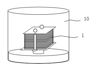
[0039] See Figure 1a In this embodiment, the tubular static PECVD method is used to form the masking film, and the single crystal silicon layer 1 is placed in the plasma deposition chamber 10 to deposit the masking film. The specific process is as follows:

[0040] a. Surface texturing

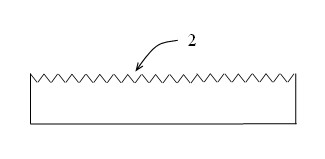
[0041] See Figure 2a , pre-cleaning the incoming single-crystal bare silicon wafer 12, the pre-cleaning adopts ultrasonic waves, and adds a certain amount of cleaning and decontaminating agent. Afterwards, the silicon wafer is placed in a sodium hydroxide solution with a temperature of 75-80°C and a mass percentage concentration of 1%-2% for surface texturing, and an appropriate amount of texturing catalyst is added to make the silicon wafer with a 100-crystal orientation A uniform "py...

Embodiment 2

[0054] Figure 1b It is a structural schematic diagram of the plate machine used in the present invention. In this embodiment, the masking film is produced by a plate-type PECVD static method. The specific process is as follows:

[0055] a. Surface texturing

[0056] See Figure 2a , pre-cleaning the incoming single-crystal bare silicon wafer 12, the pre-cleaning adopts ultrasonic waves, and adds a certain amount of cleaning and decontaminating agent. Afterwards, the bare silicon wafer 12 is placed in a sodium hydroxide solution with a temperature of 75-80°C and a mass percent concentration of 1%-2% for surface texturing, and an appropriate amount of texturing catalyst is added to achieve a texture in the 100-crystal orientation. A uniform "pyramid" textured structure 2 with a size of 1-3um is formed on the surface of the silicon wafer, so that the surface has a good light-trapping effect.

[0057] b. Fabrication of Diffusion Masking Film

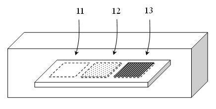
[0058] see next Figure 2b Pl...


PUM

PropertyMeasurementUnit
Thicknessaaaaaaaaaa
Thicknessaaaaaaaaaa

Abstract

The invention discloses a preparation method of a solar cell. The method comprises the following steps: providing a plurality of polycrystalline silicon wafers for texturization; overlapping the textured silicon wafers, depositing a silicon nitride or silicon oxide masking film on the periphery of the silicon wafers, then diffusing a phosphorus doping layer on the front surface of the to-be-prepared positive electrode of the silicon wafers to form a PN junction, wherein the periphery of the silicon wafers can not form the diffusion PN junction owning to the existence of the masking film; removing the peripheral masking film and the surface phosphosilicate glass; preparing a passivation layer and an antireflection layer; and performing screen printing and sintering to form a back Ag electrode, a back Al-back surface and a front Ag electrode. In the preparation method of the solar cell provided by the invention, the masking film is formed before the impurity source diffusion used for preparing the PN junction; owning to the existence of the masking film, the periphery of the silicon wafers can not form the PN junction; and the silicon wafers after diffusion is washed with acid to remove the masking film on the periphery of the silicon wafers and the phosphosilicate glass on the diffusion surface, thus achieving the aim of replacing the etching step.

Description

technical field [0001] The invention relates to a method for manufacturing a semiconductor element, in particular to a method for preparing a solar cell, and belongs to the technical field of solar cell production. Background technique [0002] At present, the production process of conventional silicon solar cells is as follows: surface pre-cleaning, texturing to remove the damaged layer and form an anti-reflection textured structure, chemical cleaning and drying; the method of liquid source diffusion forms uniform doping at each point on the surface of the silicon wafer. Remove the peripheral PN junction and surface phospho-silicate glass formed during the diffusion process; deposit passivation and anti-reflection film on the surface; make the back electrode, back electric field and front electrode of the solar cell; sinter to form an ohmic contact, thus completing the entire battery film making process. Among them, the step of removing the peripheral PN junction formed d...

Claims


Application Information

Patent Timeline
IPC IPC(8): H01L31/18
CPCY02P70/50
Inventor 石劲超
Owner 百力达太阳能股份有限公司
Why Eureka
Try Eureka