

Sedimentation growing method of semiconductor nanocrystalline/quantum dots on single crystal silicon material
A growth method and technology of quantum dots, which are applied in semiconductor devices, sustainable manufacturing/processing, photovoltaic power generation, etc., can solve the problems of narrow crystalline silicon energy band, increase production cost, sunlight loss, etc., achieve easy industrial application, improve Utilization efficiency, stable effect of physicochemical properties
- Summary
- Abstract
- Description
- Claims
- Application Information
AI Technical Summary
Problems solved by technology
Method used
Image

Examples
Embodiment 1
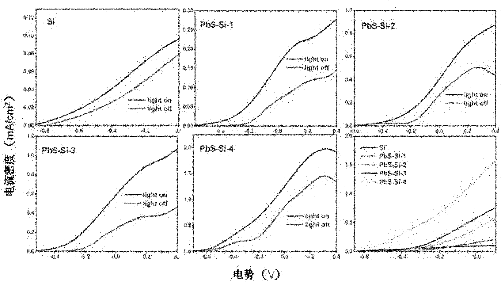
[0041] The specific steps of the preparation method of the quantum dot-sensitized Si solar cell provided in this example are as follows: a) Dissolve 1.8 g of lead acetate in 8 ml of oleylamine, heat to 120° C. for 30 min, and evacuate with argon for 3 min.
[0042] b) Dissolve 0.023g of sulfur in 6mL of oleic acid, stir and heat to 80°C for 10min.
[0043] c) Inject the sulfur solution into the metal salt solution and keep it warm for 1 min, take it out, disperse it with n-hexane and oleic acid at a ratio of 1:2, centrifuge, remove the upper layer solution, re-disperse it with n-hexane, centrifuge once, and dry it.
[0044] d) Dissolving the quantum dots in n-hexane for later use.
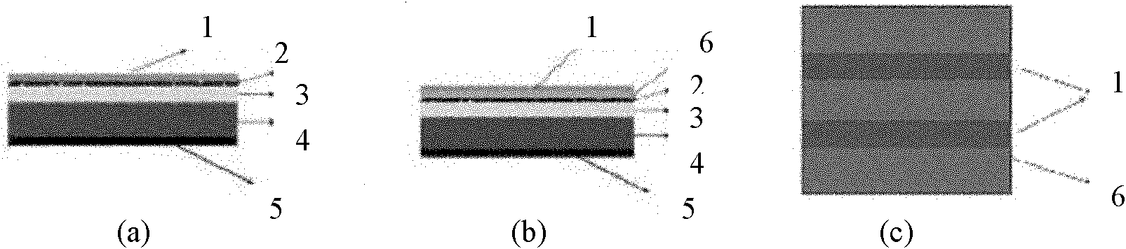
[0045] e) Put the diffusion-treated monocrystalline silicon wafer into the solvent for 30 minutes, take it out, and treat it in vacuum at 250° C. for 2 hours.
[0046] f) The single crystal silicon wafer after the diffusion treatment is put into a solvent and pulled at 5 cm / s, repeated 15 times, a...
Embodiment 2
[0050] The preparation method of this example is the same as that described in Example 1, except that in step a), 1.8 g of lead acetate is dissolved in 5 ml of oleylamine, heated at 120° C. for 30 minutes, and evacuated with argon for 3 minutes.
Embodiment 3
[0052] The preparation method of this example is the same as that described in Example 1, except that in step a), 1.8 g of lead acetate is dissolved in 12 ml of oleylamine, heated at 120° C. for 30 minutes, and evacuated with argon for 3 minutes.
PUM
| Property | Measurement | Unit |
|---|---|---|
| thickness | aaaaa | aaaaa |
| particle diameter | aaaaa | aaaaa |
| conversion efficiency | aaaaa | aaaaa |
Abstract
Description
Claims
Application Information