

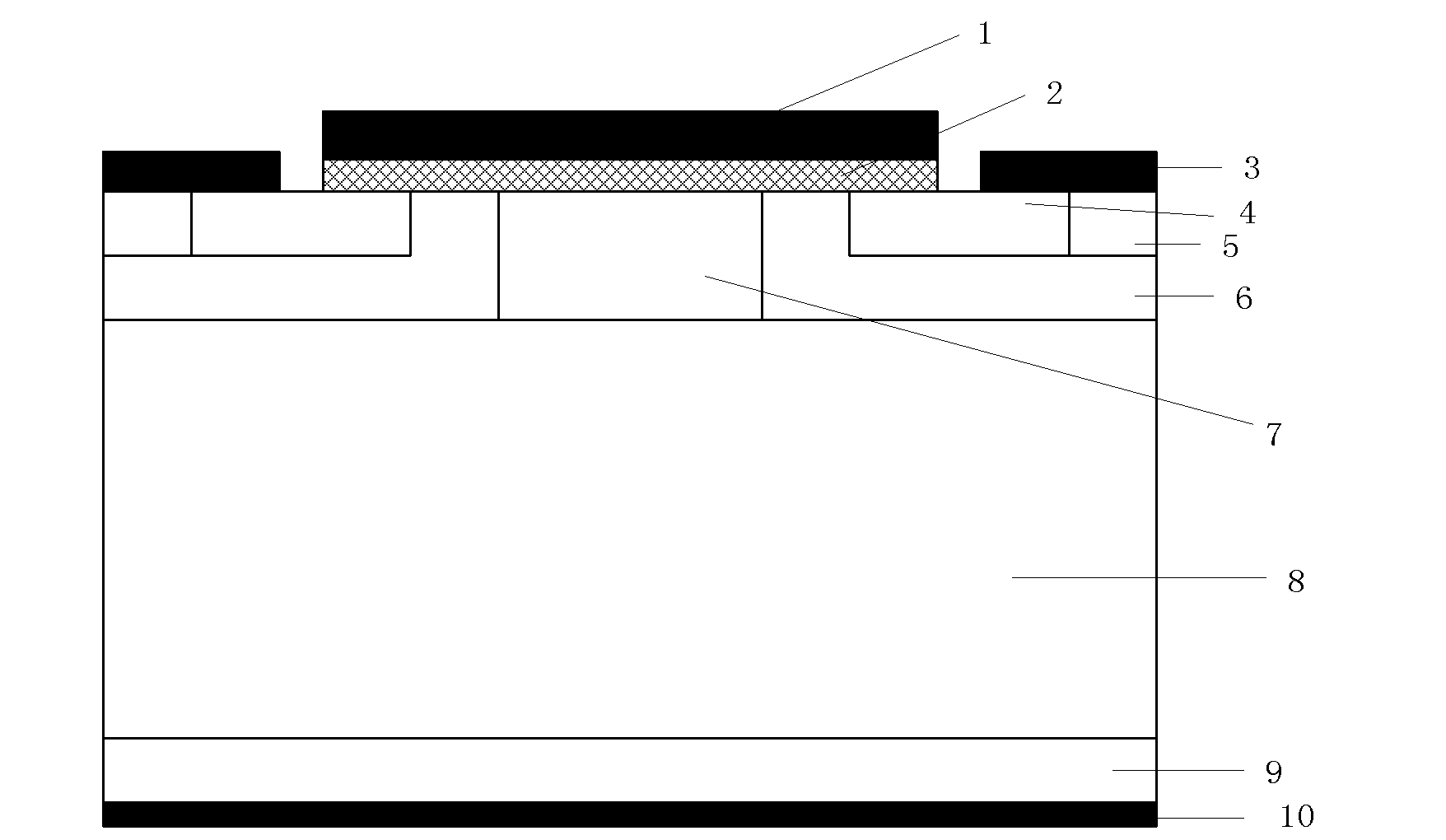
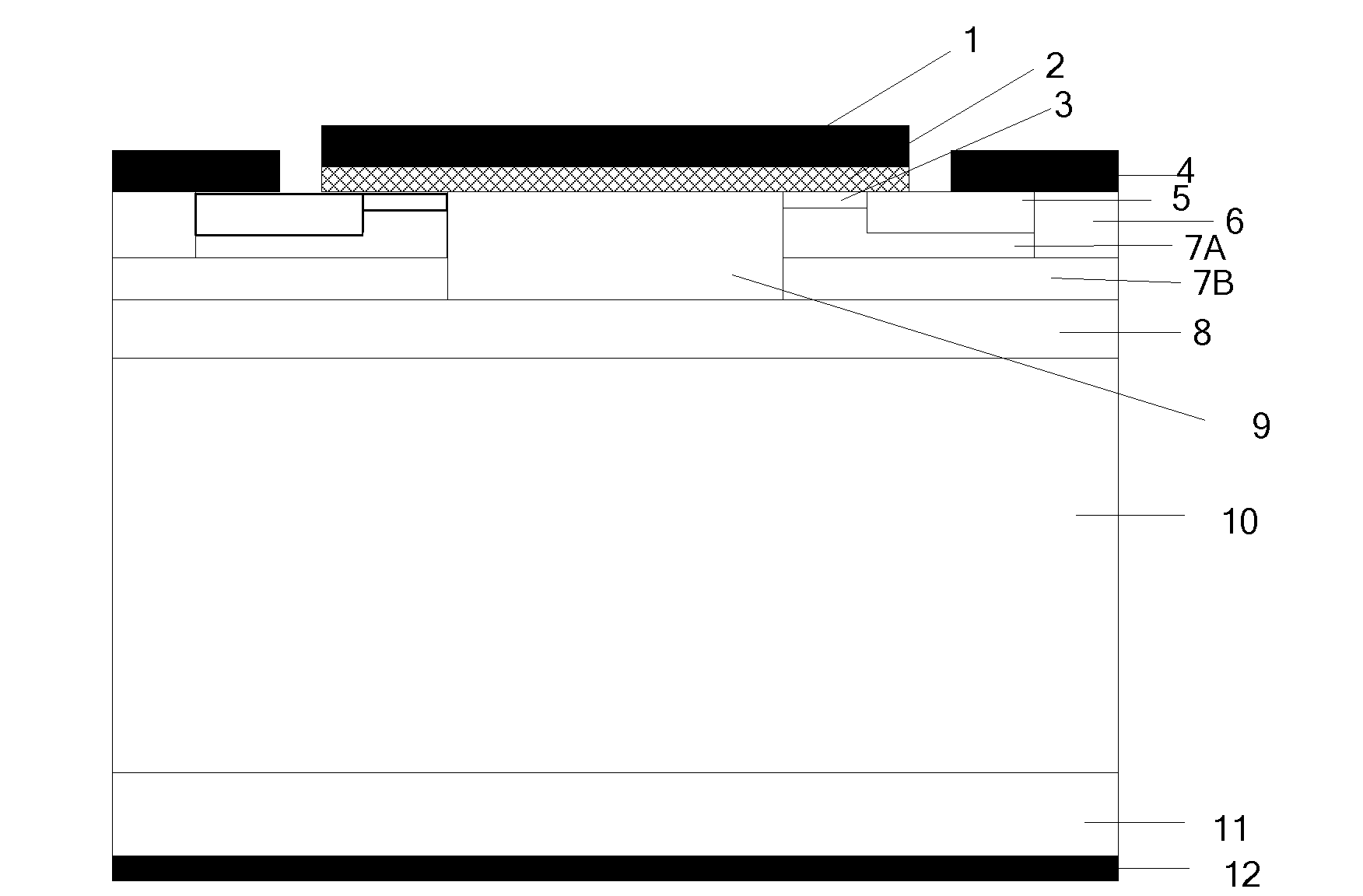
N-type buried-channel silicon carbide metal oxide semiconductor field effect transistor (DEMOSFET) device and preparation method thereof
An N-type, buried technology, applied in the field of microelectronics, can solve the problems of weakening the withstand voltage capability of devices, and achieve the effects of increasing breakdown voltage, reducing on-resistance, and increasing area
- Summary
- Abstract
- Description
- Claims
- Application Information
AI Technical Summary
Problems solved by technology
Method used
Image

Examples
Embodiment 1
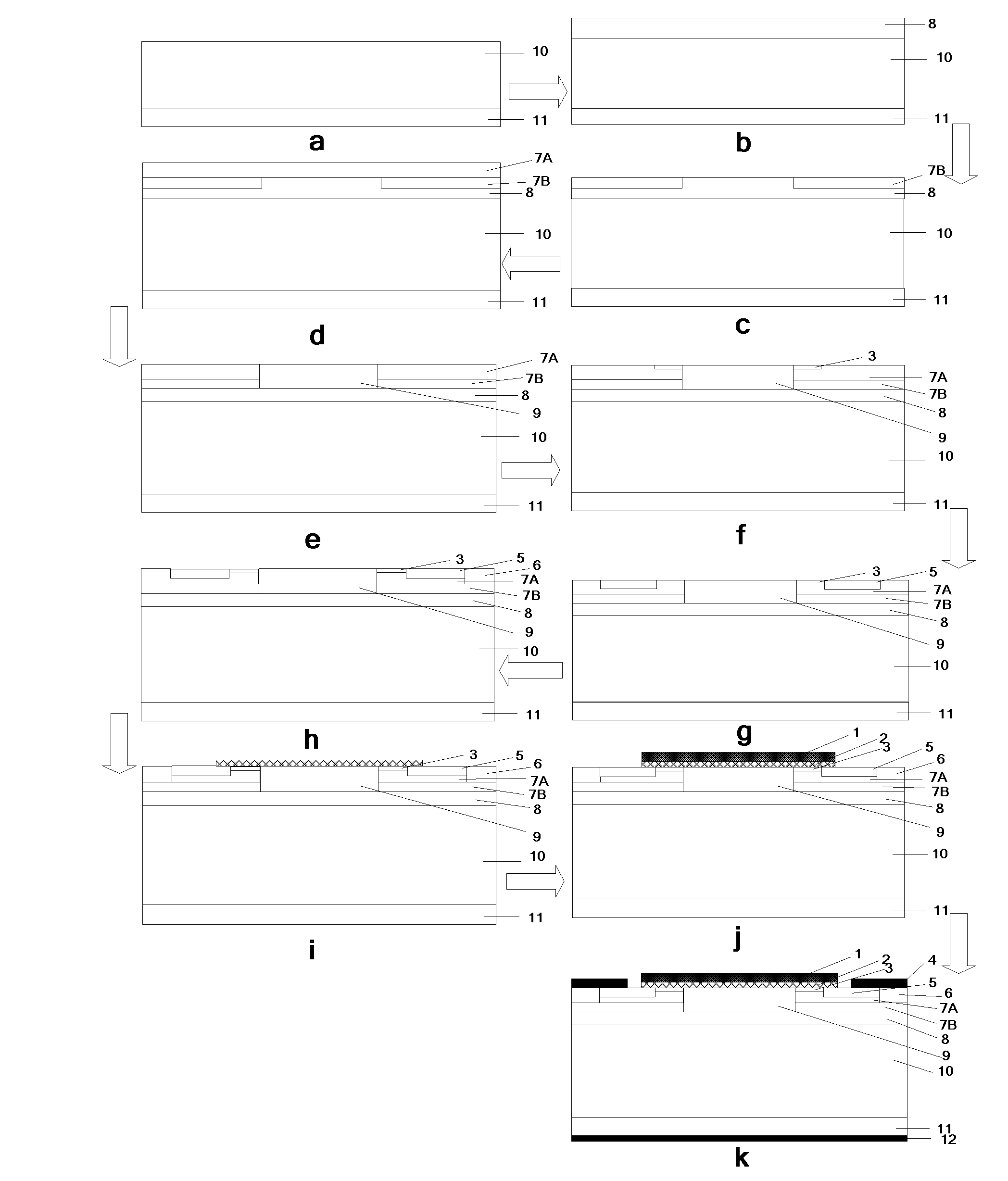
[0036] Step 1, at N + Epitaxial growth of N on SiC substrate - drift layer, such as image 3 a.
[0037] First to N + Type silicon carbide substrate 11 is cleaned by RCA standard; and then epitaxially grown on the front surface with a low-pressure hot-wall chemical vapor deposition method with a thickness of 9 μm and a nitrogen ion doping concentration of 5×10 15 cm -3 N - For the epitaxial drift layer 10, the epitaxial process conditions are as follows: the temperature is 1600° C., the pressure is 100 mbar, the reaction gas is silane and propane, the carrier gas is pure hydrogen, and the impurity source is liquid nitrogen.
[0038] Step 2, at N - Epitaxial growth of the current spreading layer on the drift layer, such as image 3 b.
[0039] On the N-type drift layer 10, the epitaxial growth thickness is 0.6 μm and the nitrogen ion doping concentration is 5×10 by the low pressure hot wall chemical vapor deposition method. 16 cm -3 The epitaxial process conditions of...
Embodiment 2
[0071] Step 1, at N + Epitaxial growth of N on SiC substrate - drift layer, such as image 3 a.
[0072] First to N + Type silicon carbide substrate 11 is cleaned by RCA standard; and then epitaxially grown on the front surface with a low-pressure hot-wall chemical vapor deposition method with a thickness of 9.5 μm and a nitrogen ion doping concentration of 8×10 15 cm -3 N - For the epitaxial drift layer 10, the epitaxial process conditions are as follows: the temperature is 1600° C., the pressure is 100 mbar, the reaction gas is silane and propane, the carrier gas is pure hydrogen, and the impurity source is liquid nitrogen.
[0073] Step 2, at N - Epitaxial growth of the current spreading layer on the drift layer, such as image 3 b.
[0074] On the N-type drift layer 10, the epitaxial growth thickness is 0.55 μm and the doping concentration of nitrogen ions is 8×10 by low pressure hot wall chemical vapor deposition method. 16 cm -3 The epitaxial process conditions...
Embodiment 3
[0106] Step A, at N + Epitaxial growth of N on SiC substrate - drift layer, such as image 3 a.
[0107] First to N + Type silicon carbide substrate 11 is cleaned by RCA standard; and then epitaxially grown on the front surface with a low-pressure hot-wall chemical vapor deposition method with a thickness of 10 μm and a nitrogen ion doping concentration of 1×10 16 cm -3 N - For the epitaxial drift layer 10, the epitaxial process conditions are as follows: the temperature is 1600° C., the pressure is 100 mbar, the reaction gas is silane and propane, the carrier gas is pure hydrogen, and the impurity source is liquid nitrogen.
[0108] Step B, at N - Epitaxial growth of the current spreading layer on the drift layer, such as image 3 b.
[0109] On the N-type drift layer 10, the epitaxial growth thickness is 0.5 μm and the nitrogen ion doping concentration is 1×10 by the low pressure hot wall chemical vapor deposition method. 17 cm -3 The epitaxial process conditions o...
PUM
| Property | Measurement | Unit |
|---|---|---|
| Thickness | aaaaa | aaaaa |
| Thickness | aaaaa | aaaaa |
| Thickness | aaaaa | aaaaa |
Abstract
Description
Claims
Application Information