A kind of preparation method of mems atomic vapor chamber and atomic vapor chamber

A vapor cavity and atomic technology, applied in the field of micro-electromechanical systems, to achieve the effect of reducing light loss, improving light transmittance, and being easy to implement

Active Publication Date: 2011-11-30
江苏智能微系统工业技术股份有限公司
View PDF6 Cites 47 Cited by
  • Summary
  • Abstract
  • Description
  • Claims
  • Application Information

AI Technical Summary

Problems solved by technology

[0006] The invention proposes a preparation method of an atomic vapor chamber using MEMS technology and the atomic vapor chamber, which solves the key problem that the atomic state preparation needs to encapsulate alkali metal ...

Method used


Image

  • A kind of preparation method of mems atomic vapor chamber and atomic vapor chamber
  • A kind of preparation method of mems atomic vapor chamber and atomic vapor chamber
  • A kind of preparation method of mems atomic vapor chamber and atomic vapor chamber

Examples


Embodiment 1

[0103] A specific implementation steps of a MEMS atomic vapor single-chamber preparation method:

[0104] (1) Sample Selection

[0105] Select Pyrex glass-silicon-Pyrex glass material matching, wherein Pyrex glass sheet 18 and Pyrex glass sheet 20 are double-sided polished, and silicon wafer 1 is an N-type silicon wafer with a thickness of 500 μm polished on both sides.

[0106] (2) Sample cleaning

[0107] Cleaning with sulfuric acid-hydrogen peroxide solution and hydrofluoric acid immersion method: first soak silicon wafer 1, Pyrex glass wafer 18 and Pyrex glass wafer 20 in sulfuric acid-hydrogen peroxide solution with a temperature of 120°C and a ratio of 10:1 for 10 minutes; then At room temperature, soak with hydrofluoric acid aqueous solution at a ratio of 1:100 for 1 minute; finally, wash with deionized water and dehydrate with absolute ethanol.

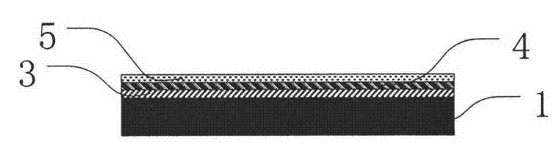
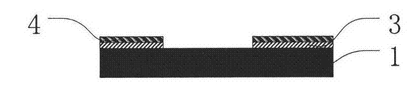
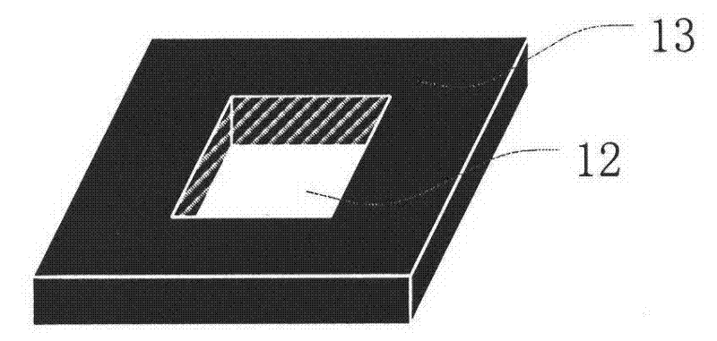
[0108] (3) Make a single-chamber space, such as figure 1 , figure 2 , image 3 shown;

[0109] The silicon wafer 1 w...

Embodiment 2

[0131] A specific implementation steps of a MEMS atomic vapor dual-chamber preparation method:

[0132] (1) Sample Selection

[0133] Pyrex glass-silicon-Pyrex glass material matching is selected, wherein Pyrex glass sheet 19 and Pyrex glass sheet 21 are double-sided polished, and silicon wafer 2 is an N-type silicon wafer with a thickness of 500 μm polished on both sides.

[0134] (2) Sample cleaning

[0135] Cleaning with sulfuric acid-hydrogen peroxide solution and hydrofluoric acid immersion method: first soak the silicon chip 2, the Pyrex glass chip 19 and the Pyrex glass chip 21 in a sulfuric acid-hydrogen peroxide solution with a temperature of 120°C and a ratio of 10:1 for 10 minutes; then At room temperature, soak with hydrofluoric acid aqueous solution at a ratio of 1:100 for 1 minute; finally, wash with deionized water and dehydrate with absolute ethanol.

[0136] (3) Make a double-chamber space, such as Figure 8 , Figure 9 , Figure 10 , Figure 12 , Figur...


PUM

PropertyMeasurementUnit
Thicknessaaaaaaaaaa

Abstract

The invention relates to a preparation method for a micro-electro-mechanical system (MEMS) atomic vapor chamber and the atomic vapor chamber. The chamber is prepared by bonding a Pyrex glass sheet, a silicon wafer and a Pyrex glass sheet by an anodic bonding technology; the Pyrex glass sheet is taken as a window of the chamber; a chamber space is formed by etching or corroding the silicon wafer; paraffin packaged alkali metal such as rubidium (Rb) or cesium (Cs) is put into the chamber, and buffer gas with appropriate pressure is introduced simultaneously; paraffin is taken as a packaging material of the alkali metal, so that active alkali metal is isolated from oxidants such as oxygen, water vapor and the like in an environment; the paraffin is also used as a plating material of the chamber, so that collision between Rb or Cs atoms and a chamber wall is slowed down; and a CO2 laser is used for melting the paraffin to release the alkali metal, so that a uniform paraffin plating is formed on the chamber wall. The problem of long-term drift caused by reaction residues generated by a field preparation mode is solved, the collision between the Rb or Cs atoms and the chamber wall is slowed down, and the contrast of atomic resonance line width of the alkali metal is improved.

Description

technical field [0001] The invention relates to an atomic vapor chamber using MEMS technology and a preparation method thereof, belonging to the field of micro-electro-mechanical systems (Micro-Electro-Mechanical Systems, MEMS), in particular to a preparation and packaging process of an atomic vapor chamber with a micro-nano structure . The atomic vapor chamber can be used for MEMS atomic devices such as MEMS atomic clocks, MEMS atomic gyroscopes, and MEMS atomic magnetometers. Background technique [0002] The miniaturization and multifunctional integration of integrated circuit technology and electronic devices have promoted the rapid development of MEMS technology. MEMS uses advanced semiconductor technology and technology to integrate machinery, electronics and even systems into one chip. It has great application prospects in military defense, aerospace, information communication, biomedical and other fields. In recent years, with the development of atomic physics, sem...

Claims


Application Information

Patent Timeline
IPC IPC(8): B81C1/00B81C3/00B81B3/00
Inventor 阮勇马波陈硕尤政
Owner 江苏智能微系统工业技术股份有限公司
Why Eureka
Try Eureka