
Zinc oxide-based transparent conductive film

A transparent conductive film, zinc oxide technology, applied in the conductive layer, circuit, photovoltaic power generation and other directions on the insulating carrier, to achieve the effect of high conversion efficiency, excellent transmittance and low resistance

Inactive Publication Date: 2015-08-26
SUMITOMO CHEM CO LTD
View PDF1 Cites 6 Cited by
  • Summary
  • Abstract
  • Description
  • Claims
  • Application Information

AI Technical Summary

Problems solved by technology

However, the transparent conductive film of Patent Document 1 has improved chemical durability and transmittance in the near-infrared region, but when calculated from the sheet resistance and film thickness, the resistivity is at least 7.4×10 -4 ~8.0×10 -4 Ω?cm or so

Method used


Image

  • Zinc oxide-based transparent conductive film
  • Zinc oxide-based transparent conductive film
  • Zinc oxide-based transparent conductive film

Examples


no. 1 approach )

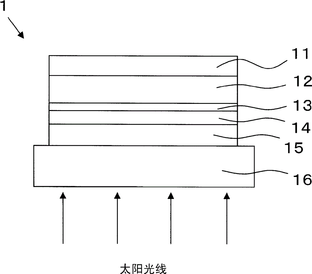
[0177] Examples of the material of the p layer include hydrogenated amorphous silicon carbide (a-SiC:H).

[0178] Examples of materials for the i layer include hydrogenated amorphous silicon (a-Si: H), crystalline silicon (c-Si), microcrystalline silicon (μc-Si), and hydrogenated amorphous silicon germanium (a-SiGe: H). . Among these, hydrogenated amorphous silicon (a-Si:H) is preferable.

[0179] In addition, examples of n-layer materials include hydrogenated amorphous silicon (a-Si:H) and microcrystalline silicon (μc-Si). Among these, hydrogenated amorphous silicon (a-Si:H) is preferable.

[0180] As another example, it is preferable to use an electrifying layer having a tandem structure in which another p-i-n layer is further formed on the p-i-n layer of a-Si. More preferably, on the layer formed on the p-i-n layer of amorphous silicon (a-Si), an a-Si:H layer as the p layer, a microcrystalline Si layer as the i layer, and a Three layers of a-Si: H layer, or a tandem str...

Embodiment 1)

[0216] Zinc oxide powder (ZnO: manufactured by Hakusitec Co., Ltd., purity 99.9%, average primary particle size 1 μm or less) and titanium monoxide powder (TiO(II): Furuuchi Chemical Co., Ltd., purity 99.9%, average primary particle size 1 μm or less) were mixed with A total of 100 g was weighed so that the atomic number ratio of zinc and titanium became Zn:Ti=98.2:1.8, and it was put into a resin bottle. Next, 50 g of ethanol was injected as a solvent, and wet mixing was performed by a wet ball mill mixing method. In this wet mixing, hard ZrO is used as balls 2 Ball (2mmφ), for 18 hours. Next, the slurry after wet mixing was taken out, the balls were removed by a sieve, the mixed solvent was removed by a rotary evaporator, and the residue was dried at 100° C. for 3 hours with a hot air dryer to obtain a mixed powder.

[0217] The obtained mixed powder was put into a mold (mold) made of graphite with a diameter of 100 mm. Vacuum pressurization was performed at a pressure of...

Embodiment 2)

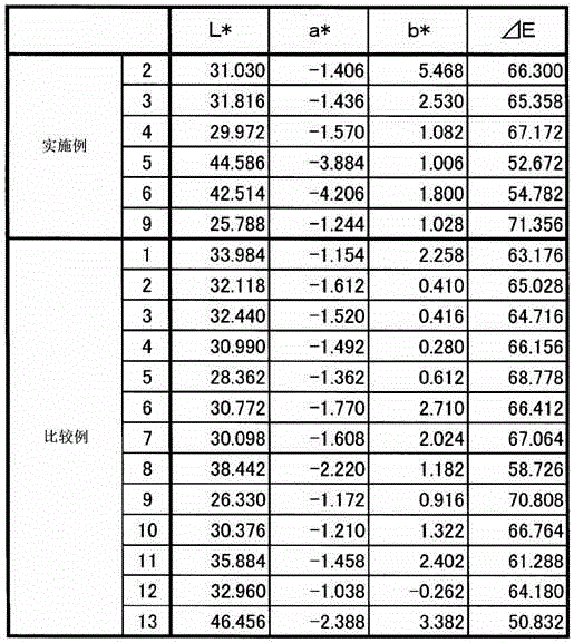
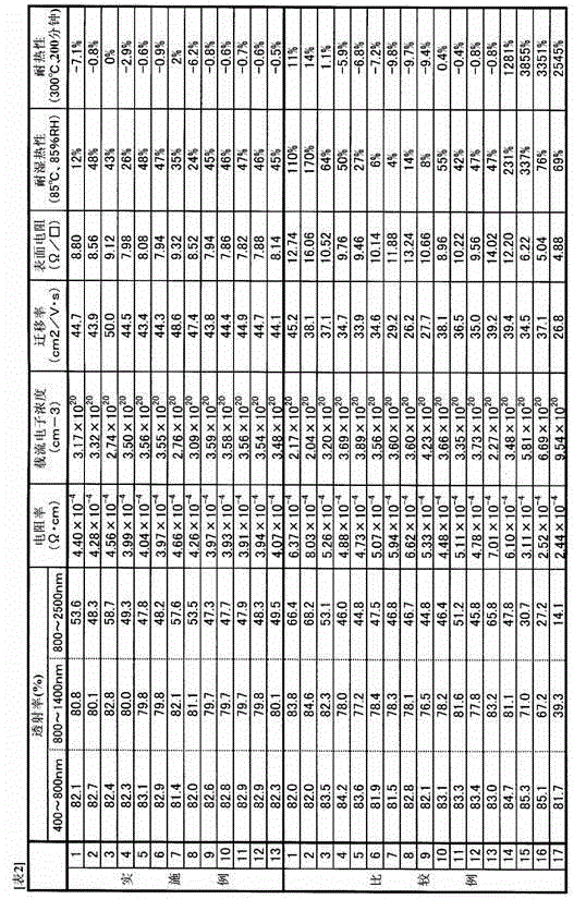
[0238] Zinc oxide powder and titanium monoxide powder were used in the same manner as in Example 1 so that the composition of the raw materials shown in Table 1 was obtained, and as the alumina powder, Sumitomo Chemical Co., Ltd. containing 99.9% purity and an average primary particle size of 0.5 μm Al made by the company 2 o 3 A sputtering target was obtained in the same procedure as in Example 1 except for the raw material powder of the powder.

[0239] Using the obtained sputtering target, a zinc oxide-based transparent conductive film was formed on the substrate to have a film thickness of about 500 nm by the sputtering method under the same conditions as in Example 1.

[0240] In the case of using any sputtering target, within about 50 minutes of sputtering, the number of times the sputtering device stops operating due to abnormal discharge is less than 3 times, the sputtering rate is about 10nm / min, and the film formation stability good.

[0241] For each obtained thi...


PUM

PropertyMeasurementUnit
melting pointaaaaaaaaaa
surface roughnessaaaaaaaaaa
densityaaaaaaaaaa

Abstract

Provided is a zinc oxide-based transparent conductive film comprising zinc atoms, oxygen atoms, and M as defined below, wherein the total number of zinc atoms, oxygen atoms, titanium atoms, gallium atoms, and aluminum atoms accounts for 99% or more of the number of all atoms forming the zinc oxide-based transparent conductive film; the ratio of the total number of titanium atoms, gallium atoms, and aluminum atoms per the total number of zinc atoms, titanium atoms, gallium atoms, and aluminum atoms contained in the film ((number of titanium atoms + number of gallium atoms + number of aluminum atoms) / (number of zinc atoms + number of titanium atoms + number of gallium atoms + number of aluminum atoms) x 100)is 1.3% or greater but 2.0% or less; the number of titanium atoms accounts for at least 50% of the total number of titanium atoms, gallium atoms, and aluminum atoms contained in the film; the carrier electron concentration is 3.60 x 1020cm-3 or less, the mobility is 43.0 cm2 / Vs or greater and resistivity is 5.00 x 10⁻⁴Ω·cm or less. M represents titanium atoms; titanium atoms and gallium atoms; titanium atoms and aluminum atoms; or titanium atoms, gallium atoms, and aluminum atoms.

Description

technical field [0001] The present invention relates to a zinc oxide-based transparent conductive film that has high transmittance in the infrared region and is useful for applications such as solar cells. Background technique [0002] Transparent conductive film is a film that has both visible light transmission and conductivity, and is used in a wide range of fields such as solar cells, liquid crystal display elements, and electrodes of light-receiving elements. As a transparent conductive film, called In 2 o 3 The ITO film in which tin oxide is added to indium oxide is manufactured and utilized by sputtering, ion plating, pulsed laser deposition (PLD), electron beam (EB) evaporation, spraying, and other film-forming methods. However, indium used as a raw material is a rare metal, and there are problems such as resource quantity and price, and a film that can replace the ITO film has been demanded. [0003] As the most effective substitute material for such an ITO film,...

Claims


Application Information

Patent Timeline
Patent Type & Authority Applications(China)
IPC IPC(8): H01B5/14C23C14/08C23C14/34H01B13/00H01L31/04H01L31/06
CPCY02E10/50G06F2203/04103C23C14/08H01L31/022483G06F3/041C23C14/086H01L31/1884C23C14/3414Y02E10/541Y02E10/548Y02P70/50
Inventor 中田邦彦堀田翔平
Owner SUMITOMO CHEM CO LTD
Learn More