

Lamination solar battery
A solar cell, solar energy technology, applied in circuits, photovoltaic power generation, electrical components, etc., can solve problems such as attenuation, battery efficiency decline, ultraviolet light-induced attenuation, etc., to achieve the effect of expanding the spectral response range
- Summary
- Abstract
- Description
- Claims
- Application Information
AI Technical Summary
Problems solved by technology
Method used
Image

Examples
Embodiment 1
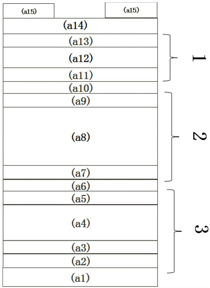
[0043] This embodiment is prepared on a 156*156mm flexible substrate, such as Figure 1a Shown:
[0044] 1. First prepare the nanocrystalline silicon (nanometer silicon germanium or amorphous silicon germanium) bottom cell, the specific steps are: prepare the first back electrode a2 on the first substrate a1, in this embodiment a1 is a polyimide film, The thickness is 50 μm. First prepare Ag thin film with a thickness ranging from 100-300nm (200nm here), the method used is thermal evaporation or sputtering, and then prepare transparent conductive thin film (ITO (indium-doped tin oxide), FTO (fluorine-doped Doped tin oxide), AZO (aluminum-doped zinc oxide), BZO (boron-doped zinc oxide), the thickness is 100-300nm (here 200nm), the preparation of this example is AZO , the method used is sputtering. Then prepare the bottom battery, first prepare the first N-type nanocrystalline silicon film a3, the method used is PECVD (plasma enhanced chemical vapor deposition), the film thick...
Embodiment 2
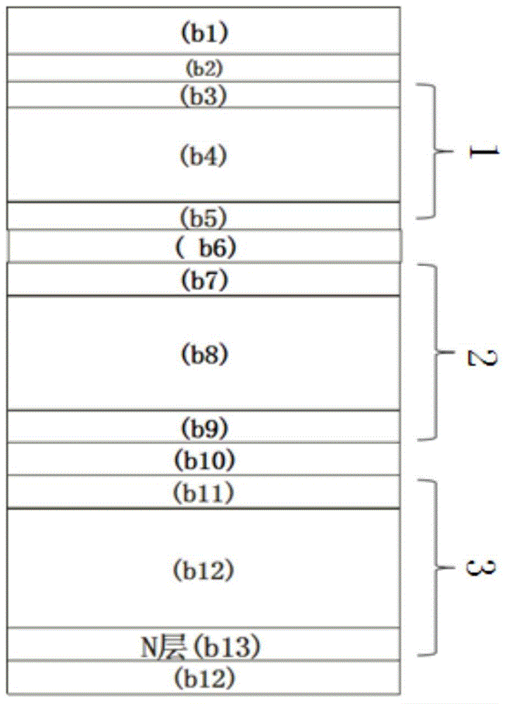
[0050] In this embodiment, the three-stack solar cell is prepared on a 156*156 glass substrate, such as Figure 1b Shown:
[0051] The second front electrode b2 is prepared on the second glass b1. In this embodiment, the front electrode is BZO with a thickness of 800 nm. The method used is LPCVD (low pressure chemical vapor deposition). After that, laser scribing P1 is used, the pitch of the scribing lines is 1 cm, and the line width is 45 μm. The laser used is 1024nm red light.
[0052] Prepare an amorphous silicon top battery afterwards, and the specific steps are: first prepare the second P-type silicon thin film layer b3, which is a P-type silicon carbide thin film in this embodiment, with a thickness of 15 nm, and the method used is PECVD, and then prepare the second non-crystalline silicon thin film layer b3. The crystalline silicon I layer b4 has a thickness of 350 nm, and the method used is PECVD. Then prepare the second N-type silicon thin film layer b5 with a thic...
Embodiment 3
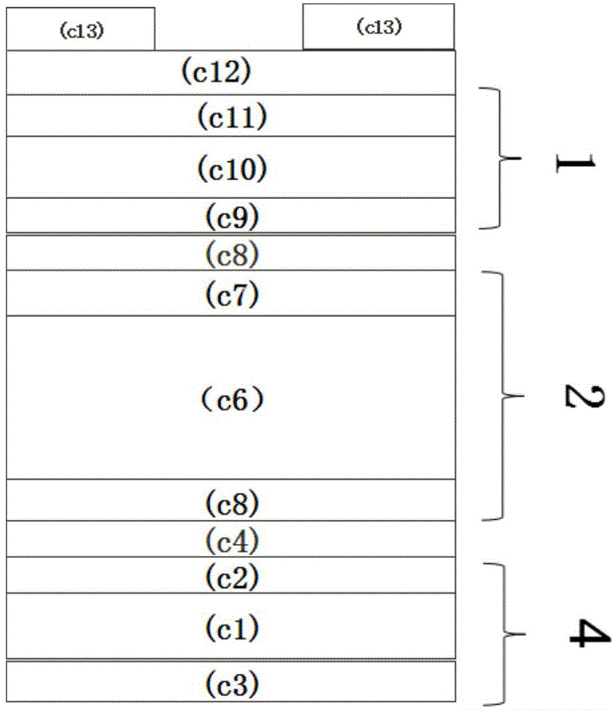
[0059] This embodiment is prepared on a 156*156N type silicon wafer. Such as Figure 2a Shown:
[0060] To prepare a crystalline silicon bottom cell, first, the third N-type silicon wafer c1 with a thickness of 150 μm is cleaned by industrial RCA, and then polished on both sides in TMAH solution, and then B (boron) is diffused to form the third P-type diffusion layer c2 The diffused sheet resistance is in the range of about 60omh / sq. Afterwards, a post-cleaning process is performed to remove the back junction, and silver-aluminum paste is printed on the side where the back junction is removed, and sintered in a sintering furnace to form the third electrode c3. Then prepare the third-intermediate layer c4. In this embodiment, the intermediate layer is ITO with a thickness of 100 nm, and the method used is sputtering.
[0061] 2. Prepare the battery in the perovskite, the specific steps are to first prepare the third electron transport layer c5, the material of the electron t...
PUM
 Abstract
Description
Claims
Application Information