GaP nanowires as well as preparation method and application thereof

A technology of nanowires and conductive substrates, applied in the direction of nanotechnology, nanotechnology, chemical instruments and methods, etc., can solve the problems of complexity, difficulty in obtaining, high price of single crystal GaP and InP substrates, and achieve uniform size and good crystallinity Effect

Active Publication Date: 2018-03-30
THE NAT CENT FOR NANOSCI & TECH NCNST OF CHINA
View PDF0 Cites 5 Cited by
  • Summary
  • Abstract
  • Description
  • Claims
  • Application Information

AI Technical Summary

Problems solved by technology

(Efficient water reduction with gallium phosphide nanowires.Nat.Commun.2015,6,7824.)(Photoelectrochemical Hydrogen Production on InP Nanowire Arrays with Molybdenum Sulfide Electrocatalysts.Nano.Lett.2014,14,3715-3719.) Nevertheless, due to single Crystalline GaP and InP substrates are expensive and difficult to obtain, while MOCVD equipment is expensive and complicated to operate, an

Method used


Image

  • GaP nanowires as well as preparation method and application thereof
  • GaP nanowires as well as preparation method and application thereof
  • GaP nanowires as well as preparation method and application thereof

Examples


Embodiment 1

[0094] This embodiment provides a preparation method of GaP nanowires, the specific method is:

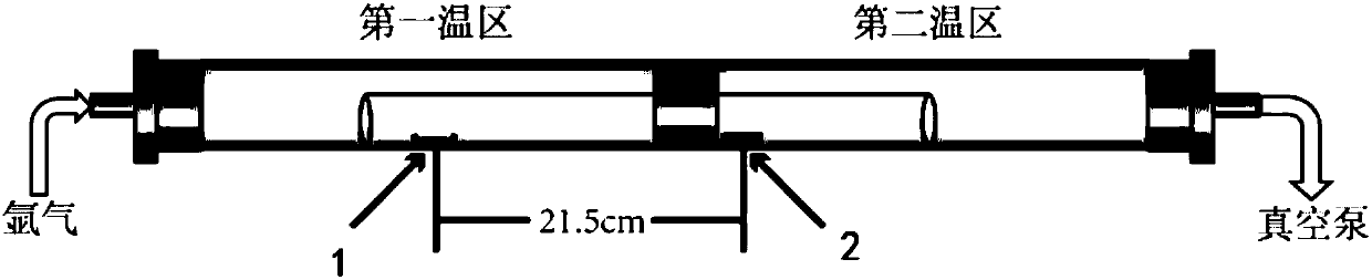
[0095] (1) Weigh about 15mg of GaP powder and put it into a quartz boat. Then the quartz boat 1 containing the GaP powder was loaded into a quartz tube with both ends opened.

[0096] (2) Cut the single-sided polished single-crystal silicon (p-type) wafer, which is the conductive substrate to grow GaP nanowires, into 1cm×1cm size, and ultrasonically clean it in acetone, isopropanol, and water for 15 minutes respectively. After the cleaned silicon substrate is blown dry with nitrogen flow, the silicon substrate 2 covered with gold film is obtained, which is placed in the chamber of the ion sputtering instrument with the polished side facing up, and the gold film is sprayed, and then it is polished from the other side of the quartz tube Put it face up into the quartz tube so that the distance from the quartz boat is 21.5 cm. Put the quartz tube into a tube furnace with two temperat...

Embodiment 2

[0104] This embodiment provides a preparation method of GaP nanowires, the specific method is:

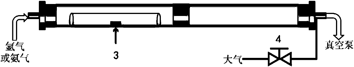
[0105] (1) Weigh about 20mg of GaP powder and put it into a quartz boat. The quartz boat is then loaded into a quartz tube that is open at both ends.

[0106] (2) The carbon cloth, the conductive substrate to be grown GaP nanowires, was cut into 1cm×1cm size, cleaned in acetone by ultrasonic for 5 minutes×3 times, followed by ultrasonic cleaning in isopropanol and water for 15 minutes respectively. After the cleaned carbon cloth substrate was blown dry with a nitrogen flow, it was fixed on a clean glass sheet, and then placed in the chamber of the ion sputtering instrument to spray-coat gold film (spray-coating twice, one on each side of the front and back). Then fix the carbon cloth base after sputtering the gold film on the quartz plate (size 1.5cm×8cm), and then put the quartz plate into the quartz tube from the other side of the quartz tube, so that the distance between the ca...

Embodiment 3

[0113] This embodiment provides a method for preparing GaP / GaPN core-shell nanowires, the specific method is:

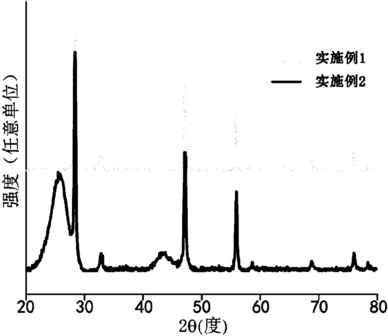
[0114] (1) Take an appropriate amount of homemade acidified KI / I 2 The solution is packed in a beaker, and the GaP nanowire sample grown on a silicon substrate prepared according to the method of Example 1 is immersed in the solution, taken out after 4 minutes, and the sample is cleaned immediately with deionized water, and then the sample is washed with nitrogen flow. Blow dry to obtain the pretreated GaP nanowire sample 3. Acidified KI / I 2 KI, I in solution 2 The mass ratio with water is 4:1:40, concentrated hydrochloric acid and by KI, I 2The volume ratio of the solution formed with water is 1:9.

[0115] (2) Put the pretreated GaP nanowire sample 3 into a quartz tube, and put the quartz tube into a tube furnace with two temperature zones, so that the sample is located in the center of the first temperature zone. The specific placement positions of the quartz...


PUM

PropertyMeasurementUnit
The average diameteraaaaaaaaaa
Lengthaaaaaaaaaa
Limiting currentaaaaaaaaaa

Abstract

The invention provides GaP nanowires as well as a preparation method and application thereof. The preparation method of the GaP nanowires comprises the following steps: 1) covering a conductive substrate with a catalyst; 2) putting GaP powder into a container; 3) placing the conductive substrate and the container at two sides of a quartz tube with openings at two ends, and putting the obtained quartz tube into a dual-temperature zone tubular furnace; and 4) vacuumizing the dual-temperature zone tubular furnace, introducing a protective gas, performing heating to make the temperature of a firsttemperature zone raised to 930 DEG C-1000 DEG C and the temperature of a second temperature zone raised to 620 DEG C-650 DEG C, and performing heat preservation to obtain the GaP nanowires. The invention also provides GaP/GaPN core-shell nanowires; and the preparation method of the GaP/GaPN core-shell nanowires comprises the following steps: placing the GaP nanowires in a quartz tube with openings at two ends, putting the obtained quartz tube into a reaction furnace, performing vacuumizing, introducing a protective gas, heating the reaction furnace, raising the temperature to 720 DEG C-800 DEG C, stopping vacuumizing and stopping introducing the protection gas, introducing an ammonia gas, and performing heat preservation to obtain the core-shell nanowires. The nanowirs provided by the invention are used as photoelectrodes.

Description

technical field [0001] The invention belongs to the field of semiconductor materials and nanotechnology, and in particular relates to a GaP nanowire and its preparation method and application. Background technique [0002] With the increasingly prominent problem of energy shortage, the research on new energy sources is gradually attracting the attention of researchers at home and abroad. The use of semiconductor materials to absorb sunlight and apply photoelectrochemical water splitting to hydrogen production is one of the solutions to energy problems. However, III-V materials have always been one of the suitable choices for photoelectrochemical electrodes due to their suitable bandgap width and excellent carrier transport properties. [0003] As early as 1998, John A.Turner and others used GaInP 2 As a photocathode for photoelectrochemical water splitting, a hydrogen production efficiency of 12.4% was achieved. (A monolithic photovoltaic-photoelectrochemical device for h...

Claims


Application Information

Patent Timeline
IPC IPC(8): C30B29/40C30B29/60C30B23/08C30B31/06C23C14/06C23C14/22C23C14/34B82Y40/00B82Y30/00
CPCB82Y30/00B82Y40/00C23C14/0617C23C14/22C23C14/34C30B23/08C30B29/40C30B29/60C30B31/06
Inventor 董泽健宫建茹
Owner THE NAT CENT FOR NANOSCI & TECH NCNST OF CHINA
Why Eureka
Try Eureka