Preparation method of interface-enhanced high-light-heat-stabilized perovskite film
A technology of interface enhancement and perovskite, which is applied in the direction of photovoltaic power generation, semiconductor/solid-state device manufacturing, semiconductor devices, etc., can solve the problems of perovskite film decomposition, poor conductivity, and charge interface accumulation, etc., to improve various properties, Effect of grain size increase and thin film defect reduction
- Summary
- Abstract
- Description
- Claims
- Application Information
AI Technical Summary
Problems solved by technology
Method used
Image
Examples
Embodiment 1
[0029] A method for preparing a perovskite film, the steps are as follows:
[0030] (1) Wash the FTO conductive glass with deionized water, acetone, absolute ethanol, and isopropanol in sequence for 15 minutes;
[0031] (2) Dry the cleaned FTO conductive glass in the air, and then perform UV ozone treatment for 15 minutes;
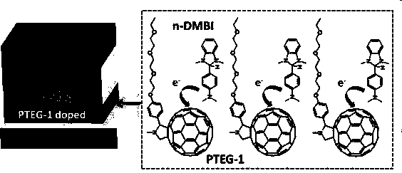
[0032] (3) Prepare a fullerene derivative chlorobenzene solution with a concentration of 20mg / mL;
[0033] (4) Add an N-type organic dopant accounting for 3% of the mass of the fullerene derivative into the chlorobenzene solution obtained in step (3), and stir uniformly;
[0034] (5) The solution obtained in step (4) is spin-coated on FTO conductive glass;
[0035] (6) The substrate is dried at room temperature (no further thermal annealing is required) to form a fullerene derivative film;
[0036] (7) Preparation of perovskite film CH 3 NH 3 PbI 3 : After step (6), the FTO conductive glass is placed in the glove box; the CH 3 NH 3 I (1.25 M), PbI 2 (1.25 M) dissolve...
Embodiment 2
[0047] In order to further verify the technical effects before and after the addition of N-type organic dopants, on the basis of the perovskite films obtained in Example 1 and Comparative Example 1, a perovskite solar cell was further fabricated. The steps are as follows:
[0048] Step S1—According to the method of Example 1 or Comparative Example 1, that is, adding and not adding N-type organic dopants to prepare perovskite films on the substrate respectively;
[0049] Step S2--The hole transport layer is prepared by the spin coating process: the hole transport layer solution ratio is 144.6 mg Spiro-OMeTAD, 58 μL tetra-tert-pyridine, and 35 μL bis(trifluoromethanesulfonyl) 520 mg / mL The acetonitrile solution of lithium amide was mixed with 2ml of chlorobenzene, and spin-coated for 30 seconds at a rotation speed of 3000 rpm;
[0050] Step S3—Prepare the metal electrode gold by vacuum thermal evaporation process, the specific parameters are: the initial pressure is 3.5×10 -7 Torr, the...
Embodiment 3
[0054] The difference from Example 1 is that the fullerene derivative is replaced with: [6,6]-phenyl-C71-isomethyl butyrate, and the N-type organic dopant is replaced with: 1, 3-Dimethyl-2-phenyl-2,3-dihydro-1H-benzimidazole, other steps remain unchanged.
[0055] The photo-thermal stability of the perovskite film can also be greatly improved, and the efficiency and stability of the corresponding battery can be greatly improved.
PUM
 Abstract
Description
Claims
Application Information


