Laser diode based on gallium nitride single-crystal substrate and preparation method of laser diode

A laser diode, gallium nitride single crystal technology, applied in lasers, laser parts, semiconductor lasers, etc., can solve problems such as difficulty in meeting, optical confinement factor, insufficient quantum efficiency, low quantum efficiency, etc., to alleviate piezoelectricity. Effects of polarization field, improved current spreading, and improved luminous efficiency

Active Publication Date: 2020-01-24
DONGGUAN UNIV OF TECH
View PDF10 Cites 10 Cited by
  • Summary
  • Abstract
  • Description
  • Claims
  • Application Information

AI Technical Summary

Problems solved by technology

However, the current quantum efficiency of GaN-based lasers is low, and further improvements are needed in terms of lifetime, reliability, and stability.
Chinese patent application 201610183087.X discloses a green laser epitaxial wafer with a stress-regulated waveguide layer. The substrate of the green laser epitaxial wafer is GaN, and its optical confinement factor and quantum efficiency are not high enough to meet the current needs.

Method used


Image

  • Laser diode based on gallium nitride single-crystal substrate and preparation method of laser diode
  • Laser diode based on gallium nitride single-crystal substrate and preparation method of laser diode
  • Laser diode based on gallium nitride single-crystal substrate and preparation method of laser diode

Examples


Embodiment 1

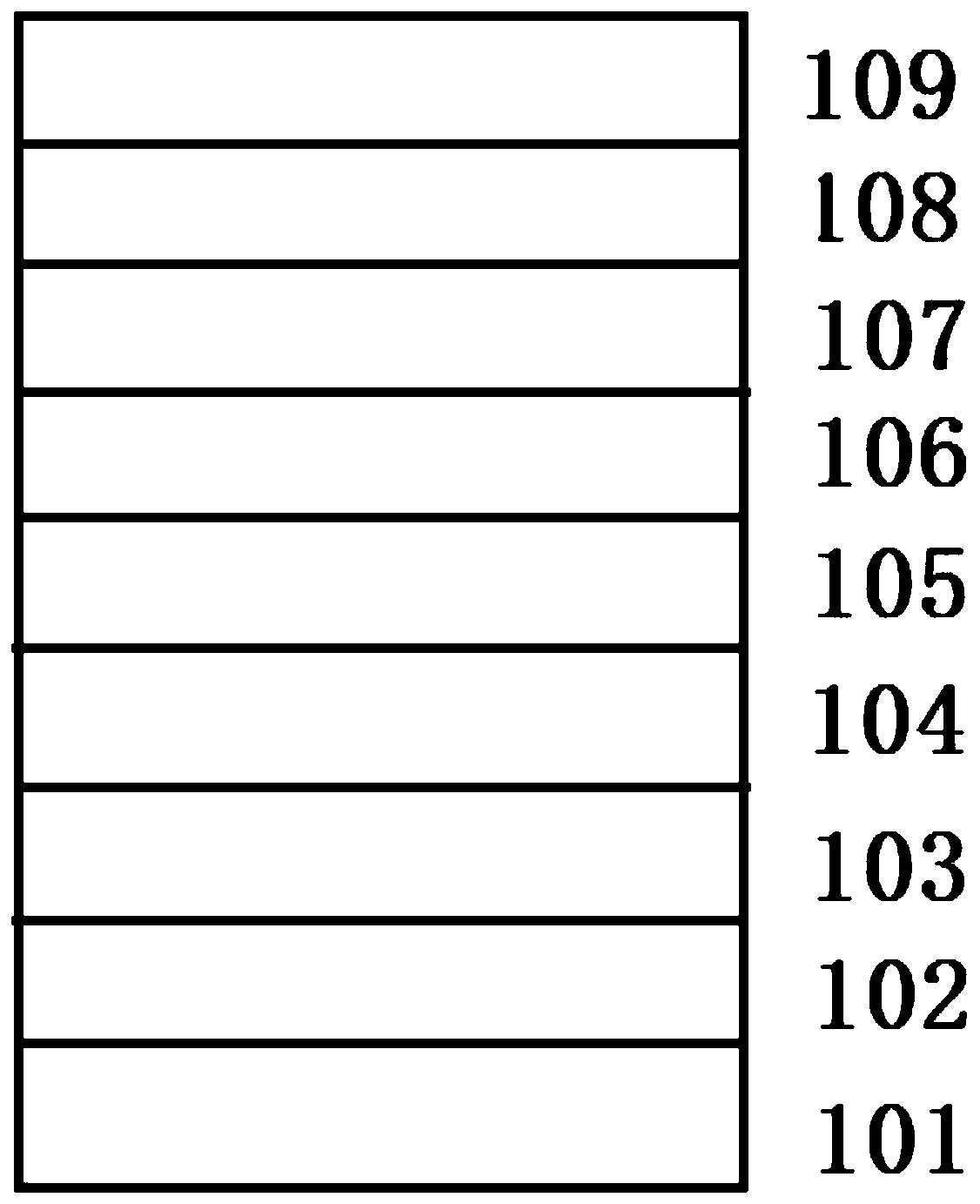
[0046] A laser diode based on GaN single crystal substrate, such as figure 1 As shown, it includes GaN single crystal substrate 101, n-type GaN layer 102, n-type confinement layer 103, lower waveguide layer 104, composite quantum well active region 105, electron blocking layer 106, upper waveguide layer 107 , p-type confinement layer 108 and p-type GaN layer 109 .

[0047] The laser diode is prepared through the following preparation steps:

[0048] S1. First, in the metal organic compound vapor phase epitaxy reaction chamber, in a hydrogen atmosphere, the temperature is raised to 500-700°C, and then ammonia gas is introduced to form a mixed atmosphere of hydrogen and ammonia, and then the temperature is raised to 900-1100°C. The single crystal substrate is subjected to surface activation treatment for 3-15 minutes.

[0049] S2. In a hydrogen atmosphere, at a temperature of 950-1200°C, feed trimethylgallium as the source of Group III, ammonia as the source of Group V, SiH 4...

Embodiment 2

[0068] This embodiment is the second embodiment of the laser diode based on gallium nitride single crystal substrate of the present invention, such as figure 1 As shown, it includes GaN single crystal substrate 101, n-type GaN layer 102, n-type confinement layer 103, lower waveguide layer 104, composite quantum well active region 105, electron blocking layer 106, upper waveguide layer 107 , p-type confinement layer 108 and p-type GaN layer 109 .

[0069] The laser diode is prepared through the following preparation steps:

[0070] S1. First, in the metal organic compound vapor phase epitaxy reaction chamber, in a hydrogen atmosphere, the temperature is raised to 500-700°C, and then ammonia gas is introduced to form a mixed atmosphere of hydrogen and ammonia, and then the temperature is raised to 900-1100°C. The single crystal substrate is subjected to surface activation treatment for 3-15 minutes.

[0071] S2. In a hydrogen atmosphere, at a temperature of 950-1200°C, feed tr...


PUM

PropertyMeasurementUnit
thicknessaaaaaaaaaa
thicknessaaaaaaaaaa
thicknessaaaaaaaaaa

Abstract

The invention discloses a laser diode based on a gallium nitride single crystal substrate and a preparation method of the laser diode. The laser diode comprises the GaN single-crystal substrate, an n-type GaN layer, an n-type limiting layer, a lower waveguide layer, a composite quantum well active region, an electron blocking layer, an upper waveguide layer, a p-type limiting layer and a p-type GaN layer which are sequentially stacked from bottom to top. According to the invention, the high-quantum efficiency stress regulation and control active region structure, the novel optical waveguide layer structure and the novel limiting layer structure of the gallium nitride-based laser diode are designed and optimized; the laser diode is prepared on the low-dislocation-density GaN single-crystalsubstrate; the technical difficulty of epitaxial preparation of a GaN-based laser is eliminated; and a GaN-based laser with high reliability and high quantum efficiency can be obtained.

Description

technical field [0001] The invention relates to the technical field of laser diodes, and more specifically, to a laser diode based on a gallium nitride single crystal substrate and a preparation method thereof. Background technique [0002] Group III-V nitride semiconductor materials are the third-generation semiconductor materials after silicon and gallium arsenide, including gallium nitride (GaN), aluminum nitride (AlN), indium nitride (InN) and their alloys , is a direct bandgap semiconductor, which has the advantages of large band gap (range 0.7-6.2eV), high breakdown electric field, high thermal conductivity, high electron saturation rate, strong radiation resistance and chemical corrosion resistance. These advantages in optoelectronic properties make III-V nitride materials have a strong competitive advantage in the field of optoelectronics (such as LED and LD), and are in an irreplaceable position. They are ideal materials for semiconductor lasers from ultraviolet to ...

Claims


Application Information

Patent Timeline
Patent Type & Authority Applications(China)
IPC IPC(8): H01S5/34H01S5/343H01S5/20
CPCH01S5/20H01S5/2009H01S5/34H01S5/3425H01S5/34333
Inventor 贾传宇凌东雄王红成吕伟王春华康晓娇胡西多
Owner DONGGUAN UNIV OF TECH
Why Eureka
Try Eureka