Plasma etching apparatus member having improved plasma-resistant properties and manufacturing method therefor

An etching device and plasma technology, which is applied in the field of plasma characteristics, can solve the problems of uneconomical ratios of different types of elements, and achieve simple deposition and heat treatment, minimized possibility of process parameter changes, and reasonable time.

Pending Publication Date: 2020-06-05
KOMICO
View PDF5 Cites 1 Cited by
  • Summary
  • Abstract
  • Description
  • Claims
  • Application Information

AI Technical Summary

Problems solved by technology

[0017] However, the plasma-resistant members of the above-mentioned prior art documents also have the limitations of the above-mentioned spraying method and other process technologies, or are mixed with different types of elements and then heated and melted to produce doped quartz glass members. , which is not economical in terms of the proportion of different kinds of elements

Method used


Image

  • Plasma etching apparatus member having improved plasma-resistant properties and manufacturing method therefor
  • Plasma etching apparatus member having improved plasma-resistant properties and manufacturing method therefor
  • Plasma etching apparatus member having improved plasma-resistant properties and manufacturing method therefor

Examples


Embodiment 1 to 3

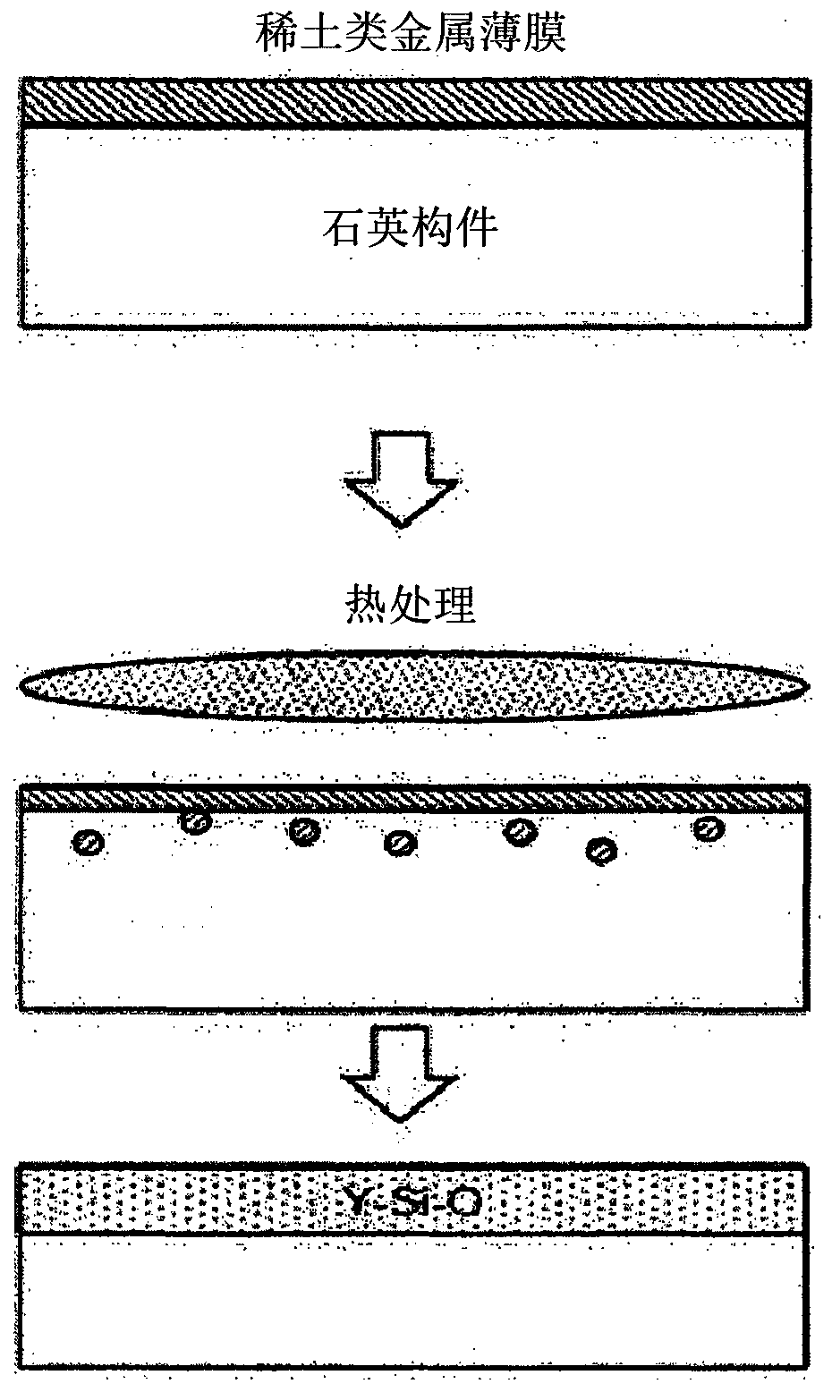
[0076] Examples 1 to 3 Yttrium metal thin films were produced under the configuration and conditions described in Table 1 below.

[0077] [Table 1]

[0078]

[0079] In order to analyze the element distribution of the examples, the following experiments were performed.

experiment example 1- 2

[0080]

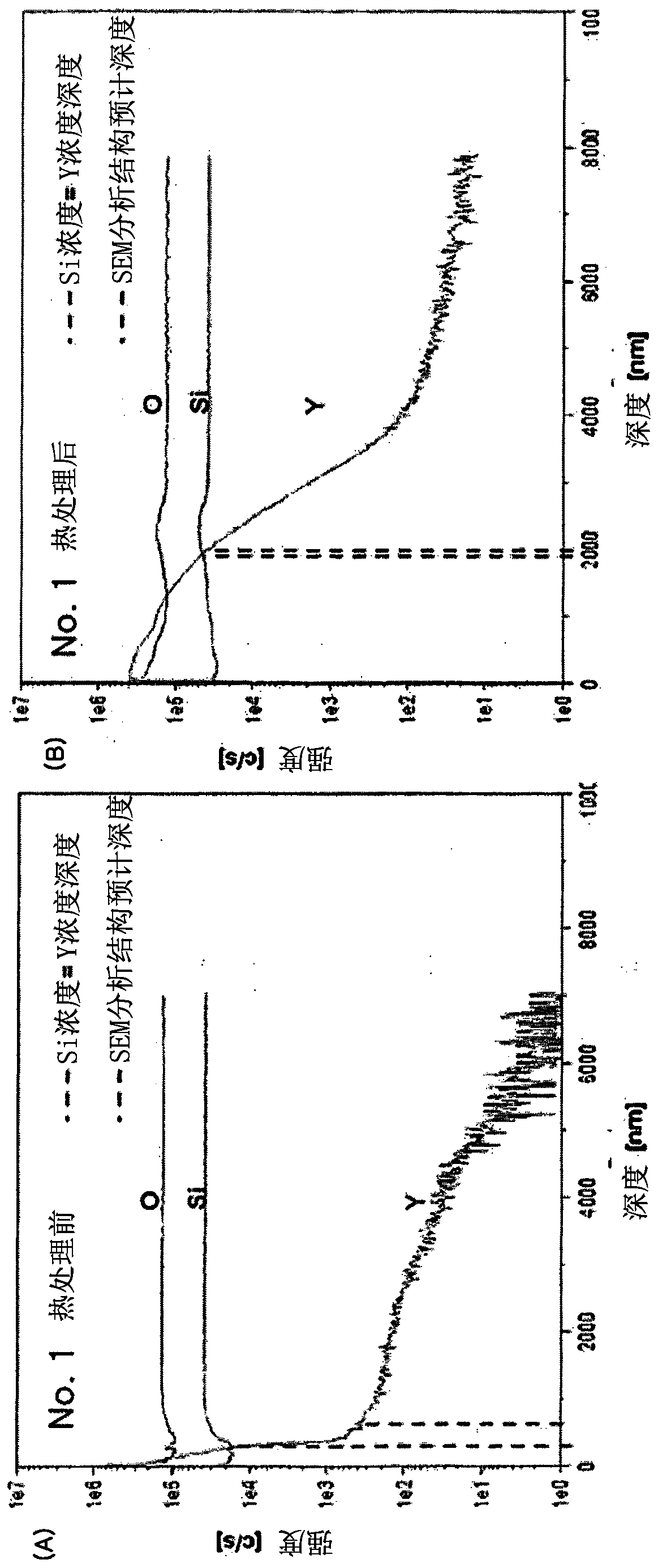
[0081] The depth of thermal diffusion of the yttrium (Y) element in Examples 1 and 2 was evaluated using a secondary ion mass spectrometer (hereinafter referred to as "SIMS"). First, in order to minimize the exposure of the sample protective film to the atmosphere, the sample is placed in a purge system, a part of the protective film of the sample is collected, and added to the SIMS analysis sample holder (sample holder). While maintaining a purge state, place the sample rack in the preparation chamber of the SIMS device, pump the preparation chamber, and place it in the experimental chamber. ), using an oxygen ion gun (oxygen ion gun), quantitative analysis of yttrium (Y), silicon (Si) and oxygen (O) content, to obtain a depth profile graph (depth profile graph).

[0082] The depth curves of Example 1 and Example 2 are shown in image 3 and Figure 4 . This takes into consideration that the positive ionization characteristics of each element are superior to the...

experiment example 2

[0086]

[0087] Using X-ray photoelectron spectroscopy (XPS) (Thermo Fisher Scientific, using Al Kα (1486.6eV) X-ray light source), the chemical bonding state and atomic content of the test pieces before and after plasma treatment were investigated. The basic pressure of the test piece chamber is adjusted to 10 -9 Torr, in the analysis, holds 10 -9 ~10 -7 support range. The measured spectrogram is displayed as a plot of electron binding energy versus electron number for a fixed, small-energy interval. Peak area and peak height sensitivity coefficients were used for quantification. All surface compositions shown here are expressed in atomic % (atm%).

[0088] like Figure 5 As shown, the Y three-dimensional orbit shows Y 3d3 / 2 and 3d5 / 2 peaks by means of L-S coupling. When yttrium oxides are formed, 3d oxide peaks are generated at lower binding energy positions due to chemical shifts. exist Figure 5 In (B), the Y 3d oxide peak appears on the surface after heat treatme...


PUM

PropertyMeasurementUnit
melting pointaaaaaaaaaa
thicknessaaaaaaaaaa
thicknessaaaaaaaaaa

Abstract

The present invention relates to a plasma etching apparatus member and a manufacturing method therefore, and more specifically, relates to the plasma etching apparatus member, which improves plasma-resistant properties through deposition of rare earth metal thin film and surface heat treatment, and maintains the light transmittance so as to be usable as a member for analyzing the end point of an etching process, and the manufacturing method therefor.

Description

technical field [0001] The present invention relates to a member for a photoplasma etching device and a manufacturing method thereof, and more specifically, relates to a technique for improving the plasma resistance of a member for a plasma etching device by utilizing a thermal diffusion phenomenon of a rare earth metal thin film. Background technique [0002] In the semiconductor manufacturing process, the importance of the plasma dry etching process tends to become more and more important for the microfabrication required for the high integration of substrate circuits such as silicon wafers. [0003] Since the plasma etching process can make the vertical etching rate much larger than the horizontal etching rate, the final aspect ratio of the etched pattern can be appropriately controlled. If a plasma etching process is actually used, an extremely fine pattern having a large aspect ratio in a film having a thickness of about 1 micron can be formed. [0004] The chamber env...

Claims


Application Information

Patent Timeline
Patent Type & Authority Applications(China)
IPC IPC(8): H01L21/3065H01L21/324H01L21/02
CPCH01L21/3065H01L21/02H01J37/32642C23C14/5806C23C16/4404C23C14/564C23C14/18H01J37/32477H01L21/324H01L21/02631C23C14/185C23C14/30C23C14/34H01J2237/0203H01J2237/334H01L21/67069
Inventor 郑洞勳高贤哲金善台
Owner KOMICO
Why Eureka
Try Eureka