Wide-range pressure sensor chip and monolithic integration preparation method thereof

A pressure sensor and monolithic integration technology, applied in the field of MEMS sensors, can solve problems such as difficulty in adapting to pressure detection, difficulty in ensuring repeatability and consistency, and small pressure measurement range of pressure sensors

Pending Publication Date: 2021-09-10
杭州电子科技大学温州研究院有限公司 +1
View PDF0 Cites 3 Cited by
  • Summary
  • Abstract
  • Description
  • Claims
  • Application Information

AI Technical Summary

Problems solved by technology

However, the sensitive film in this pressure sensor chip is prepared by wet etching, and its repeatability and consistency are difficult to guarantee, which is not conducive

Method used


Image

  • Wide-range pressure sensor chip and monolithic integration preparation method thereof
  • Wide-range pressure sensor chip and monolithic integration preparation method thereof
  • Wide-range pressure sensor chip and monolithic integration preparation method thereof

Examples


Embodiment 1

[0066] The specific steps of a monolithic integrated preparation method for a wide-range pressure sensor chip are as follows:

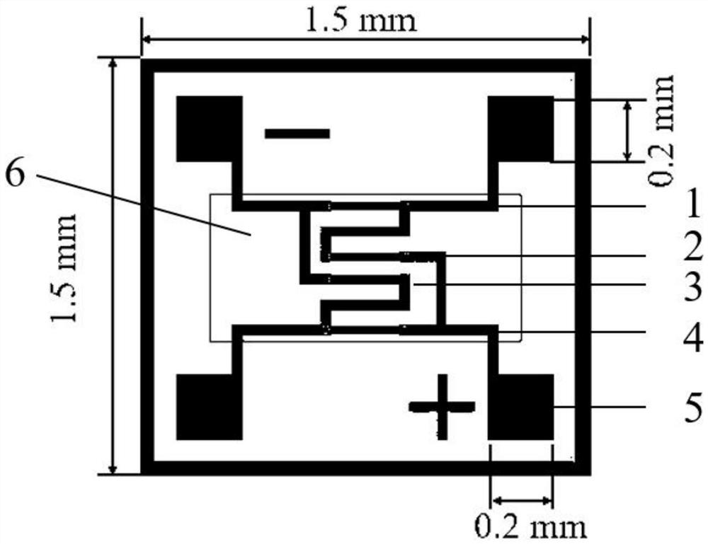
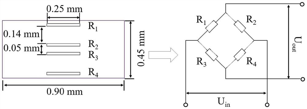
[0067] S1: Using SOI as the substrate, using photolithography, ion implantation, plasma enhanced chemical vapor deposition (PECVD), reactive ion etching (RIE), spin coating, evaporative deposition, wet etching and stripping and other micromachining processes to form Planar structures such as piezoresistive (1, 2, 3, 4), pads and interconnection lines (5) and passivation layer (7);

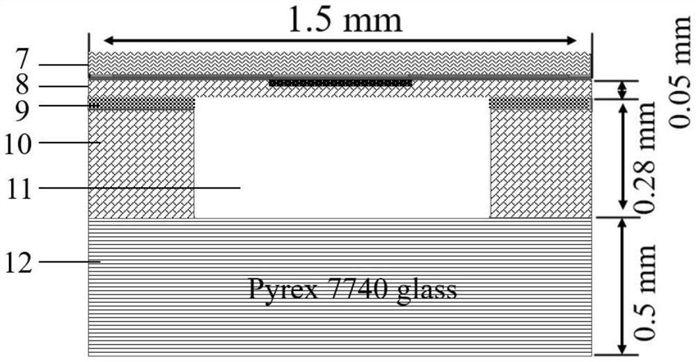
[0068] S2: Use double-side alignment photolithography, deep silicon etching on the back, RIE etching of the buried oxide layer, and silicon-glass anode bonding process on the back to form the back chamber of the pressure sensor.

[0069] The specific process of step S1 is as follows:

[0070] 1) if Pic 4-1 As shown, using an SOI silicon wafer as a substrate, the SOI was ultrasonically cleaned in acetone, ethanol, and deionized water for 5 minutes, dried with nitrogen, a...

Embodiment 2

[0086] The specific steps of a monolithic integrated preparation method for a wide-range pressure sensor chip are as follows:

[0087] S1: Using SOI as the substrate, using photolithography, ion implantation, plasma enhanced chemical vapor deposition (PECVD), reactive ion etching (RIE), spin coating, evaporative deposition, wet etching and stripping and other micromachining processes to form Planar structures such as piezoresistive (1, 2, 3, 4), pads and interconnection lines (5) and passivation layer (7);

[0088] S2: Use double-side alignment photolithography, deep silicon etching on the back, RIE etching of the buried oxide layer, and silicon-glass anode bonding process on the back to form the back chamber of the pressure sensor.

[0089] The specific process of step S1 is as follows:

[0090] 16) Using an SOI silicon wafer as a substrate, ultrasonically clean the SOI in acetone, ethanol, and deionized water for 5 minutes, dry it with nitrogen, and bake it on a hot plate a...


PUM


Abstract

The invention discloses a wide-range pressure sensor chip and a monolithic integration preparation method thereof. An existing pressure sensor chip has low linearity and sensitivity and a narrow range. The invention relates to monolithic micromachining preparation of a piezoresistive pressure sensor. The pressure sensor is mainly composed of a vacuum chamber, a pressure sensitive film and a Wheatstone bridge formed by four piezoresistors, wherein the pressure sensitive film is composed of a silicon film and a polyimide film; on one hand, the novel silicon-polyimide composite pressure sensitive film can enlarge the measurement range of the pressure sensor by increasing the film thickness, and on the other hand, the sensitivity and linearity of the pressure sensor can be improved through the combination of rigidity and flexibility. When the external pressure changes, the common deformation of the silicon film and the polyimide film causes the resistance value change of the piezoresistor and enables the output voltage of the Wheatstone bridge to change.

Description

technical field [0001] The invention belongs to the technical field of MEMS sensors, and in particular relates to a monolithic integrated preparation method for a wide range pressure sensor chip. bit integration. Background technique [0002] With the development of silicon-based micromachining technology, silicon-based pressure sensors have been well developed and widely used in industrial and commercial applications. In recent years, with the expansion of electronic device markets such as automotive, aerospace, biomedical, Internet of Things, and portable electronic devices, the development of monolithic integrated silicon-based micro-pressure sensors with multi-function, high reliability, low cost, and large-scale manufacturing capabilities Sensor chips have become a hot spot in the current consumer market. [0003] Jian Dong et al. from Zhejiang University developed a new monolithic composite MEMS sensor in the paper "Monolithic-integrated piezoresistiveMEMS accelerome...

Claims


Application Information

Patent Timeline
IPC IPC(8): B81B7/02B81C1/00
CPCB81B7/02B81C1/00134B81B2201/0264
Inventor 王高峰王明浩程瑜华
Owner 杭州电子科技大学温州研究院有限公司
Why Eureka
Try Eureka