HEMT device based on sputtering AlON/diamond substrate and preparation method thereof

A diamond and device technology, which is applied in the field of HEMT devices and its preparation, can solve the problems of difficult MOCVD direct epitaxy, poor thermal stability, and large gaps, so as to facilitate large-scale integration, improve device quality, and improve device performance. Effect

Pending Publication Date: 2022-05-24
西安电子科技大学芜湖研究院
View PDF0 Cites 0 Cited by
  • Summary
  • Abstract
  • Description
  • Claims
  • Application Information

AI Technical Summary

Problems solved by technology

[0004] However, the traditional method is easy to cause damage to the surface during the substrate peeling process. In addition, the bonding technology between diamond and GaN epitaxial layer is not mature enough, and defects are prone to occur during the bonding process, resulting in a decrease in effective thermal conductivity and poor thermal stability. Resulting in performance degradation of HEMT devices
In addition, the hexagonal structure of the diamond structure and the nitride has a large gap from the perspective of the crystal structure, and it is difficult to form direct epitaxy by MOCVD.

Method used


Image

  • HEMT device based on sputtering AlON/diamond substrate and preparation method thereof
  • HEMT device based on sputtering AlON/diamond substrate and preparation method thereof
  • HEMT device based on sputtering AlON/diamond substrate and preparation method thereof

Examples


Embodiment 1

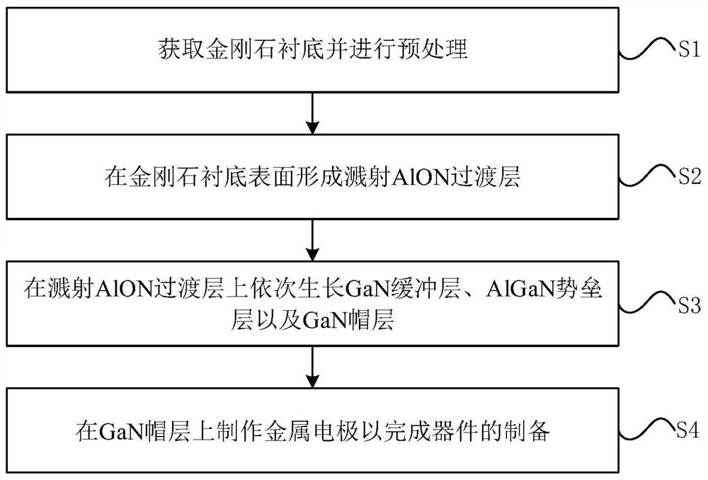
[0042] See figure 1 , figure 1 It is a schematic flowchart of a method for preparing a HEMT device based on sputtering AlON / diamond substrate provided by the embodiment of the present invention, including:

[0043] S1: Obtain a diamond substrate and perform pretreatment.

[0044] Specifically, a diamond substrate with a certain crystal orientation is selected, placed in an acetone solution, an anhydrous ethanol solution and deionized water for ultrasonic cleaning for 2-10 min each, and then dried with nitrogen.

[0045] In this embodiment, a diamond substrate is selected as the bottom plate of the device, because the high thermal conductivity of the diamond substrate can greatly improve the heat dissipation capability of the device, which is beneficial to large-scale integration.

[0046] S2: A sputtered AlON transition layer is formed on the surface of the diamond substrate.

[0047] Because the difference between the diamond material and the GaN material is too large, it ...

Embodiment 2

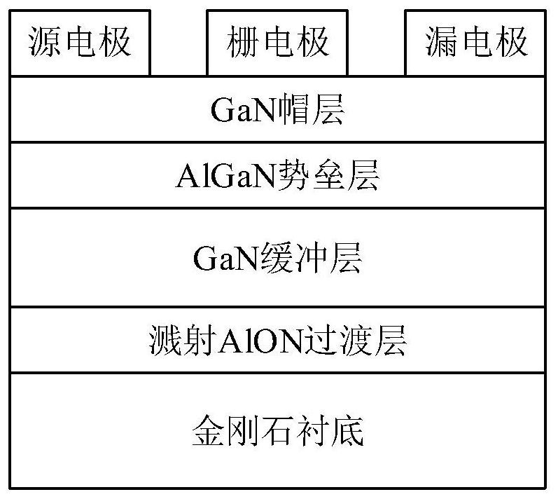
[0068] On the basis of the above-mentioned first embodiment, this embodiment provides a HEMT device based on sputtered AlON / diamond substrate. See figure 2 , figure 2 It is a schematic diagram of a HEMT device structure based on sputtered AlON / diamond substrate provided by the embodiment of the present invention. The device structure includes from bottom to top: a diamond substrate, a sputtered AlON transition layer, a GaN buffer layer, an AlGaN barrier layer, GaN cap layer, source-drain electrodes, and gate electrodes. The thickness of the AlON transition layer is 10-100 nm, the thickness of the GaN buffer layer is 1-3 μm, the thickness of the AlGaN barrier layer is 20-60 nm, and the thickness of the GaN cap layer is 2-6 nm.

[0069] The HEMT device based on the sputtered AlON / diamond substrate provided in this embodiment can be prepared by the preparation method provided in the above-mentioned Embodiment 1, and the specific preparation process is not repeated here.

Embodiment 3

[0071] Hereinafter, the preparation method provided in the above Embodiment 1 will be described in detail by taking the preparation of a GaN-based HEMT device with an AlON transition layer thickness of 10 nm as an example.

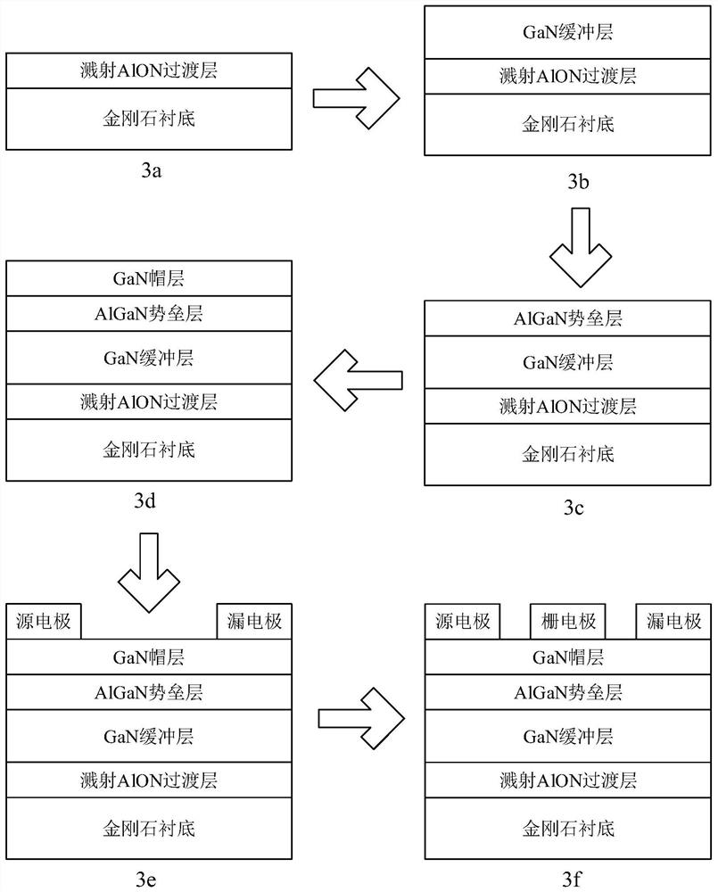
[0072] See image 3 a-3f, image 3 a-3f is a schematic diagram of the preparation process of the HEMT device based on the sputtered AlON / diamond substrate provided in the embodiment of the present invention. details as follows:

[0073] Step 1: Process the diamond substrate.

[0074] The diamond substrate was placed in acetone solution, absolute ethanol solution and deionized water for ultrasonic cleaning for 2 min each, and then dried with nitrogen.

[0075] Step 2: Sputtering the AlON transition layer.

[0076] The treated diamond substrate is put into a magnetron sputtering furnace for growth, the air pressure is 50 Torr, the sputtering power is 1000W, the flow rate of oxygen gas is 2sccm, the flow rate of argon gas is 50sccm, and the flow rate of n...


PUM

PropertyMeasurementUnit
Thicknessaaaaaaaaaa
Thicknessaaaaaaaaaa
Thicknessaaaaaaaaaa

Abstract

The invention discloses an HEMT (High Electron Mobility Transistor) device based on a sputtering AlON / diamond substrate and a preparation method of the HEMT device. The preparation method comprises the steps of obtaining a diamond substrate and performing pretreatment; forming a sputtering AlON transition layer on the surface of the diamond substrate; sequentially growing a GaN buffer layer, an AlGaN barrier layer and a GaN cap layer on the sputtering AlON transition layer; and manufacturing a metal electrode on the GaN cap layer to complete the preparation of the device. The AlON transition layer is introduced between the diamond substrate and the GaN buffer layer, so that GaN and a heterostructure thereof can be directly grown on the diamond substrate, the influence of a substrate stripping and bonding technology in a traditional method on a device is avoided, the performance of the device is improved, and the process is simple.

Description

technical field [0001] The invention belongs to the technical field of microelectronics, and in particular relates to a HEMT device based on a sputtered AlON / diamond substrate and a preparation method thereof. Background technique [0002] With the development of the microelectronics industry, ultra-wide bandgap semiconductor materials such as gallium oxide and diamond have gradually entered people's field of vision. Compared with other semiconductor materials, ultra-wide bandgap semiconductor materials theoretically have greater advantages in the application fields of extreme environments such as high temperature, strong radiation, and high current due to their larger band gaps, so they have become an international research topic. hot spot. Diamond material has the advantages of large band gap, high hardness, high melting point, stable chemical properties and good insulation, etc. It has great application potential in the fields of high frequency, high power, high temperat...

Claims


Application Information

Patent Timeline
IPC IPC(8): H01L21/335H01L29/778H01L29/06
CPCH01L29/66045H01L29/778H01L29/0603
Inventor 许晟瑞杜金娟苏华科张金风彭若诗周弘张春福张进成郝跃
Owner 西安电子科技大学芜湖研究院
Why Eureka
Try Eureka