Colloidal silicon nanocrystal with high fluorescence quantum yield as well as preparation method and application of colloidal silicon nanocrystal

A fluorescence quantum yield, colloidal silicon technology, applied in the fields of nanotechnology, nanotechnology, nanotechnology for materials and surface science, can solve the problems of low photoluminescence quantum efficiency, surface oxidation, etc., to improve Fluorescence quantum efficiency, complete surface modification, non-toxic effect of raw material cost

Pending Publication Date: 2022-07-08
SHANGHAI UNIV OF ENG SCI
View PDF1 Cites 0 Cited by
  • Summary
  • Abstract
  • Description
  • Claims
  • Application Information

AI Technical Summary

Problems solved by technology

[0006] The technical problem to be solved by the present invention is to provide a method for preparing c-Si NCs by adding HF solution in an organic solvent as a ligand for the existing technology for preparing c-Si NCs, which is easy to cause surface oxidation and low photoluminescence quantum efficiency. c-Si NCs with stable performance, narrow size distribution, adjustable size and emission wavelength, and high photoluminescence efficiency were obtained.

Method used


Image

  • Colloidal silicon nanocrystal with high fluorescence quantum yield as well as preparation method and application of colloidal silicon nanocrystal
  • Colloidal silicon nanocrystal with high fluorescence quantum yield as well as preparation method and application of colloidal silicon nanocrystal
  • Colloidal silicon nanocrystal with high fluorescence quantum yield as well as preparation method and application of colloidal silicon nanocrystal

Examples


Embodiment 1

[0039] (1) Take a 1cm×1cm single-crystal silicon wafer [thickness~350μm, p-type, (100)] that has been cleaned and dried with alcohol, deionized water, etc., put it in a sample bottle, add 15ml of toluene (>99 %) solution, put it into a magnetic stirrer, and place it on the magnetic stirrer.

[0040] (2) Pass through a titanium / sapphire laser (wavelength 800nm, pulse width 100fs, frequency 80MHz, laser energy density 0.2mJ cm) while magnetically stirring -2 ) liquid phase ablation for 60 min.

[0041] (3) The ablated sample was centrifuged at a high speed of 15,000 rpm for 3 times, and each time was 30 minutes; the upper layer solution obtained by separation was slightly turbid.

[0042] According to the above formula, the PL QY of the c-Si NCs obtained in Example 1 was 48.6%.

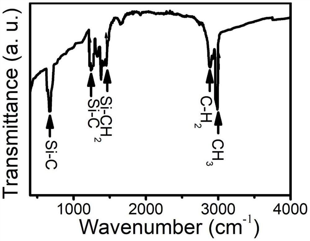
[0043]The obtained upper layer solution was characterized by structure such as XRD, XPS, FTIR, HRTEM, etc., and its optical properties such as PL, time-resolved PL, and UV-vis absorbance spectrum were...

Embodiment 2

[0045] (1) Take a 1cm×1cm monocrystalline silicon wafer same as in Example 1, put it in a sample bottle, add 15ml of mixed solvent of toluene (>99%) and HF solution, put it in a magnetic stirring bar, put it in a magnetic on the mixer. The purity of toluene used in the mixed solution is >99%; the concentration of the added HF solution is 50wt% (specific gravity 1.157), the volume percentage in the mixed solution is 5.0%, and the HF content is about 28-30g / L.

[0046] (2) Pass through a titanium / sapphire femtosecond laser (wavelength 800nm, pulse width 100fs, frequency 80MHz, laser energy density 0.2mJ cm) while magnetically stirring -2 ) liquid phase ablation for 60 min.

[0047] (3) The ablated sample was centrifuged at a high speed of 15,000 rpm for 3 times, and each time was 30 minutes; the upper layer clear liquid was obtained by separation, which was pale yellow.

[0048] The PL QY of the obtained c-Si NCs was 65.7%.

Embodiment 3

[0050] (1) Take a 1cm×1cm monocrystalline silicon wafer same as in Example 1, put it in a sample bottle, add 15ml of mixed solvent of toluene (>99%) and HF solution, put it in a magnetic stirring bar, put it in a magnetic on the mixer. The purity of toluene used in the mixed solution is more than 99%; the concentration of the added HF solution is 50wt%, the volume percentage in the mixed solution is 10.0%, and the HF content is about 57-59g / L.

[0051] (2) Pass through a titanium / sapphire femtosecond laser (wavelength 800nm, pulse width 100fs, frequency 80MHz, laser energy density 0.2mJ cm) while magnetically stirring -2 ) liquid phase ablation for 60 min.

[0052] (3) The ablated sample was centrifuged at a high speed of 15,000 rpm for 3 times, and each time was 30 minutes; the upper layer clear liquid was obtained by separation, which was pale yellow.

[0053] The PL QY of the obtained c-Si NCs was 77.2%.

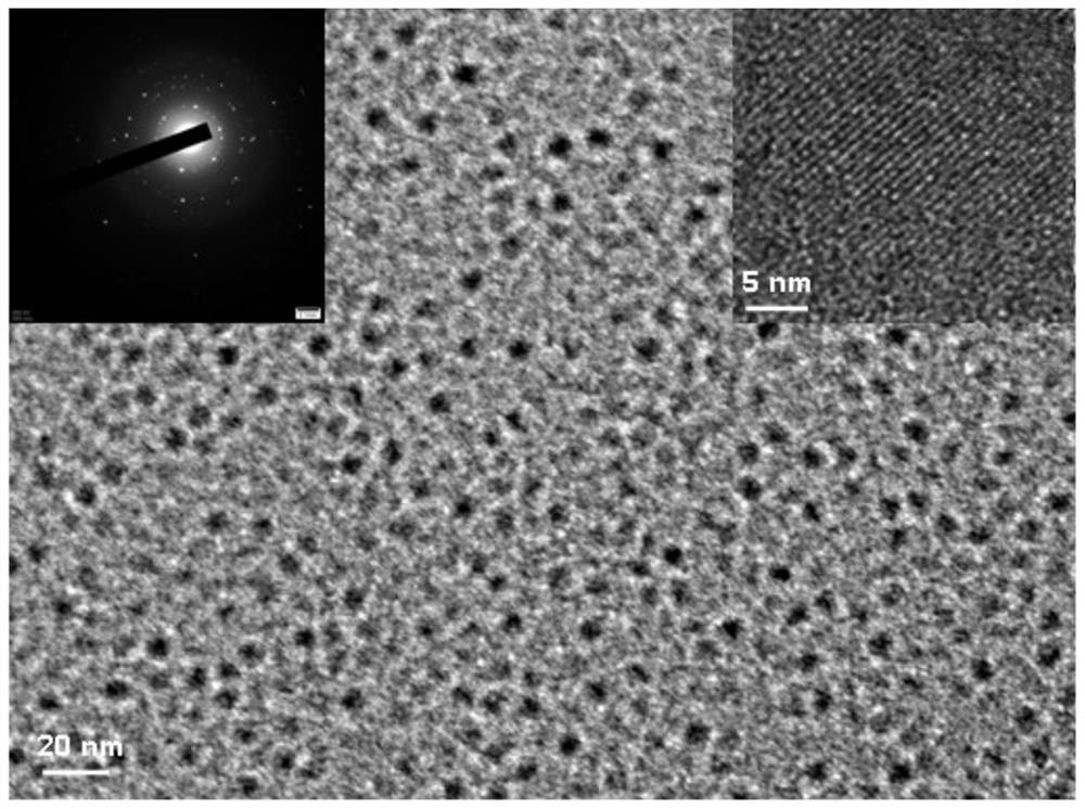
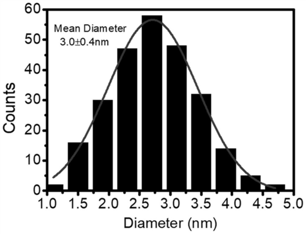
[0054] figure 1 It is a transmission electron microscope image o...


PUM

PropertyMeasurementUnit
thicknessaaaaaaaaaa
wavelengthaaaaaaaaaa
thicknessaaaaaaaaaa

Abstract

The invention relates to the field of a preparation technology of a functional nano material and application of the functional nano material to a photoelectric device, in particular to preparation of colloidal silicon nanocrystals (c-Si NCs) with high fluorescence quantum yield and application of the colloidal silicon nanocrystals (c-Si NCs) to an OLED (Organic Light Emitting Diode). According to the method, a block monocrystalline silicon wafer, an organic solvent and a hydrofluoric acid (HF) solution are mainly used for being mixed, the c-SiNCs with high fluorescence quantum efficiency, good surface functionalization and uniform dispersion are generated in one step through femtosecond laser liquid phase ablation, used consumables are low in cost, used reagents are non-toxic and free of strong corrosivity, and the c-SiNCs can be applied to the field of fluorescence imaging. The prepared c-Si NCs has the characteristics of no toxicity, high fluorescence quantum efficiency (as high as 78.5%), easiness in regulation and control of size distribution and light-emitting wavelength and the like. A c-Si NCs film is prepared from the prepared c-Si NCs solution through a one-step spin-coating method and applied to an OLED, and the external quantum efficiency can reach 7.2%. The process does not need complex chemical modification, is simple and easy to implement, has good repeatability, has good stability in amplification experiments, and is wide in industrial application prospect.

Description

technical field [0001] The invention relates to the technical field of preparation of nanomaterials, in particular to a colloidal silicon nanocrystal with high fluorescence quantum yield, a preparation method thereof and an application in the production of OLED. Background technique [0002] The Bohr radius of silicon nanocrystals (Si NCs) is less than 5.0 nm, and its quantum structure has a strong quantum confinement effect. At the same time, silicon has the advantages of high content, non-toxicity and environmental friendliness in the earth's crust. In recent years, silicon has been increasingly used in the fields of optoelectronic devices and biodetectors. Colloidal silicon nanocrystals (c-Si NCs) are driving new semiconductor nanodevices such as light-emitting diodes based on non-traditional processes in recent years due to their good solution dispersibility, luminescence stability, and ease of solution processing. S.Y.Zhao, et al. IEEE Transactions on Electron Devices ...

Claims


Application Information

Patent Timeline
Patent Type & Authority Applications(China)
IPC IPC(8): C09K11/59H01L51/54B82Y30/00B82Y40/00
CPCC09K11/59B82Y30/00B82Y40/00H10K50/115Y02P70/50
Inventor 郝惠莲赵悦
Owner SHANGHAI UNIV OF ENG SCI
Why Eureka
Try Eureka