High-resistivity single crystal zinc oxide wafer based radiation detector and preparation method and use thereof

a single crystal zinc oxide wafer and radiation detector technology, applied in the field of high-resistivity single crystal zinc oxide wafer and radiation detector, can solve the problems of limiting the application of related detectors in harsh environments and hindering their application in the field of radiation detection, and achieves low cost, simple operation, and ultra-high resistivity.

Active Publication Date: 2020-06-02
SUN YAT SEN UNIV
View PDF6 Cites 0 Cited by
  • Summary
  • Abstract
  • Description
  • Claims
  • Application Information

AI Technical Summary

Benefits of technology

[0007]The technical problem to be solved by the present invention is to overcome the shortcomings and deficiencies of the above-described prior art, providing a preparation method of high-resistivity single crystal ZnO for a radiation or photoelectric detector. This method uses an electrochemical method combined with an annealing treatment to obtain an ultra-high resistivity single crystal ZnO wafer. The preparation method is novel, simple to operate, low in cost and high in repeatability. Further, a semiconductor device for alpha particle detection is prepared based on the high-resistivity single crystal zinc oxide material. The present invention utilizes a high-resistance ZnO material having excellent characteristics such as a superior anti-irradiation capability, a wider band gap, and higher breakdown electric field strength to manufacture a radiation detector, and the obtained device exhibits a good radiation response and has a simple structure, a low cost and a high repeatability.
[0047]The present invention first provides a preparation method of high-resistivity single crystal ZnO for a radiation or photoelectric detector. This method uses an electrochemical method combined with an annealing treatment to obtain an ultra-high resistivity single crystal ZnO wafer in only two simple steps. The obtained ZnO wafer has a resistivity of up to 1011 Ωcm. Moreover, the preparation method of the present invention is novel, simple in operation, low in cost and high in repeatability, and has good promotion and application prospects.
[0049]The present invention uses a high-resistance ZnO material having excellent characteristics such as a superior anti-irradiation capability, a wider band gap, and higher breakdown electric field strength to manufacture a radiation detector. The obtained device has a simple structure, a simple manufacturing process, a low cost, a high repeatability, a high practicability, and good promotion and application prospects.
[0050]Moreover, the present invention uses the high-quality and high-resistivity ZnO single crystal as a functional material, which has strong anti-radiation capability, which determines that the device can work under strong radiation conditions such as nuclear science technical field and space.
[0051]The present invention adopts a more mature method of thermal evaporation or electron beam evaporation, which has the characteristics of uniform and controllable film thickness, ensures high electrode quality, can realize electrode evaporating of most metals, and provides a wide manufacturing space for electrode selection and control of device performance.
[0052]The present invention uses a single-energy alpha source with a low beam current as a radiation source, which can better reflect a sensitivity of the device to a detection signal, and can better reflect a discrimination of the device on detected signal energy.

Problems solved by technology

However, both silicon and germanium are sensitive to ambient temperature and weak in radiation resistance due to their narrow band gap, so it is greatly restricted to equip them into a system working in space environment.
These problems greatly limit the application of related detectors in harsh environments such as nuclear power plant and space.
However, how to obtain high resistivity and thereby strongly suppress dark current noise in order to obtain high-resistivity single crystal ZnO with high signal-to-noise ratio has been an important obstacle hindering its application in the field of radiation detection.

Method used


Image

  • High-resistivity single crystal zinc oxide wafer based radiation detector and preparation method and use thereof
  • High-resistivity single crystal zinc oxide wafer based radiation detector and preparation method and use thereof
  • High-resistivity single crystal zinc oxide wafer based radiation detector and preparation method and use thereof

Examples


embodiment 1

[0060]1. Preparation of High-Resistivity ZnO Single Crystal

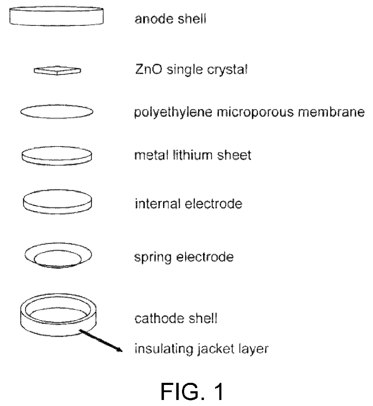
[0061](1) A high-quality low-resistance zinc oxide wafer of 10 centimeter squares was assembled into a commercial CR 2032 battery case in the order shown in FIG. 1 at room temperature in an argon-filled glove box, an electrolyte used was a 1 M LiPF6 solution dispersed in a mixed solution of ethylene carbonate, ethyl methyl carbonate and diethyl carbonate in a volume ratio of 4:3:3, and a Celgard 2400 polyethylene microporous membrane was used as an electronic diaphragm.

[0062]A LAND BT2013A multi-channel battery testing system performed a constant-current discharge treatment at room temperature to realize an injection of lithium into the ZnO single crystal.

[0063]A thickness of the high-quality low-resistance zinc oxide wafer used was 0.3 millimeters, a constant current discharge current was set to 3 μA, and a discharge time was set to 15 hours.

[0064](2) The lithium-injected zinc oxide wafer treated in the above step (1) was p...

embodiment 2

[0067]1. Preparation of high-resistivity single crystal ZnO

[0068]The method differed from Embodiment 1 in that the thickness of the ZnO wafer in the step (1) was 0.2 millimeters, the constant current discharge current was set to 3 μA, and the discharge time was set to 10 hours.

[0069]Compared with Embodiment 1, this Embodiment shortened the discharge time due to a reduction of the thickness of the wafer, thereby obtaining a same processing result.

[0070]2. The high-resistivity ZnO single crystal wafer prepared by this Embodiment had a resistivity of 1011 Ωcm, which was 1011 higher than that before treatment.

embodiment 3

[0071]1. Preparation of high-resistivity single crystal ZnO

[0072]The method differed from Embodiment 1 in that the thickness of the ZnO wafer in the step (1) was 0.5 millimeters, the constant current discharge current was set to 3 μA, and the discharge time was set to 25 hours.

[0073]Compared with Embodiment 1, this Embodiment prolonged the discharge time due to an increase in the thickness of the wafer, thereby obtaining the same processing result.

[0074]2. The high-resistivity ZnO single crystal wafer prepared by this Embodiment had a resistivity of 1011 Ωcm, which was 1011 higher than that before treatment.


PUM

PropertyMeasurementUnit
volume ratioaaaaaaaaaa
pressureaaaaaaaaaa

Abstract

The present invention discloses a high-resistivity single crystal zinc oxide (ZnO) wafer and a high-resistivity single crystal ZnO-based radiation detector, and preparation method and use thereof. The preparation method of the high-resistivity single crystal zinc oxide wafer is to place a single crystal ZnO wafer in a metal lithium electrochemical device for a constant-current discharge treatment, and then to place the single crystal ZnO wafer in a high-pressure oxygen atmosphere at 800 to 1000° C. and 10 to 30 atm for an annealing treatment for 20 to 28 hours. The preparation method of the radiation detector is to evaporate a metal electrode layer at both sides of the high-resistivity single crystal ZnO wafer, then to bond the wafer onto a circuit board, and to connect the wafer with the circuit board by a gold thread.

Description

CROSS-REFERENCE TO RELATED APPLICATION[0001]This application is a continuation of international PCT application serial no. PCT / CN2016 / 095816, filed on Aug. 18, 2016, which claims the priority benefit of China application no. 201610612939.2, filed on Jul. 29, 2016, and a continuation of international PCT application serial no. PCT / CN2016 / 095817, filed on Aug. 18, 2016, which claims the priority benefit of China application no. 201610612940.5, filed on Jul. 29, 2016. The entirety of each of the above-mentioned patent applications is hereby incorporated by reference herein and made a part of this specification.TECHNICAL FIELD[0002]The present invention belongs to the technical field of radiation detector, and more specifically, relates to a high-resistivity single crystal zinc oxide wafer and a radiation detector, and a preparation method and use thereof.BACKGROUND[0003]In many fields of military, national defense, aerospace, etc., detectors need to have characteristics such as high se...

Claims


Application Information

Patent Timeline
Patent Type & Authority Patents(United States)
IPC IPC(8): H01L21/00H01L31/08H01L31/0224H01L31/0296H01L31/02C30B33/04C30B29/16H01L31/18
CPCH01L31/02002C30B29/16H01L31/0296C30B33/04H01L31/1828H01L31/0224H01L31/085
Inventor HUANG, FENGJI, XUDONG, MEIYAN, KUN
Owner SUN YAT SEN UNIV
Why Eureka
Try Eureka